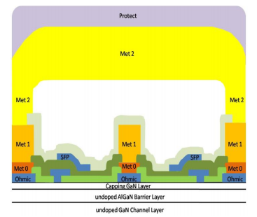
WIN Semiconductors has released an improved version of its 0.25 µm, 28 V GaN on SiC process. According to the company, the enhanced NP25 process offers 2 dB higher stable gain, increased power-added efficiency and fast switching time for discrete transistor and MMIC applications through 12 GHz. Among the improvements, WIN optimized the transistor DC and RF IV characteristics to be closer to “ideal.”
The increased device gain enables higher power density and power-added efficiency under a range of tuning and bias conditions. At 10 GHz, the NP25 process provides saturated output power of 5 W/mm of gate periphery, greater than 65 percent power-added efficiency and 19 dB linear gain.
This performance makes the NP25 process well suited for high power, linear and broadband transmit functions in radar, satellite communications and wireless infrastructure systems.
The NP25 process is fully qualified and supported with a comprehensive design kit and transistor models. Sample kits are available and can be obtained by contacting WIN’s regional sales managers.
WIN’s 4-in GaN on SiC process was first released to production in 2015 and is fabricated at the company’s wafer fab in Taiwan. Formed in 1999, WIN is the industry’s largest “pure play,” compound semiconductor foundry.

