

Figure 1 AN/APG-81 AESA radar, which flies on the F-35. Source: Northrop Grumman.
Editor's Note: This is the second of two articles in this month's radar and antennas issue that discusses architectural changes accelerating the evolution to the next-generation of phased array radar.
Digital beamforming in phased arrays has proliferated in recent years, spawned by both military and commercial applications and advancements in RF component integration. Although massive MIMO and automotive radar are the subjects of much discussion, most of the recent radar development and beamforming R&D that has been in the defense industry (see Figure 1), is now being adapted for commercial applications. While phased arrays with digital beamforming moved from R&D to reality in the 2000s, a new wave of defense systems are being developed, enabled by semiconductor technology that was previously cost prohibitive.
ANALOG vs. DIGITAL BEAMFORMING
The block diagram of a generic phased array with analog and digital beamforming is shown in Figure 2. The number of elements in the array is chosen based on aperture size, power and antenna pattern requirements. Front-end or transmit/receive (T/R) modules are located behind each antenna element, and an analog beamforming layer is behind the front-end modules. In historic phased arrays, the analog beamforming subsystem combines all the elements to centralized receiver channels. In many systems today, some level of analog beamforming is common. In a system with only digital beamforming, waveform generators and receivers are behind every front-end module, and the analog beamforming layer is eliminated. The waveform generator and receiver channels serve to convert digital data to the operating band RF frequencies. Digital beamforming is accomplished by first equalizing the channels, then applying phase shifts and amplitude weights to the analog-to-digital (A/D) data, followed by a summation of the A/D data across the array. Many beams can be formed simultaneously, limited only by the digital processing capability.

Figure 2 Generic AESA block diagram, showing analog and digital beamforming functions.

Figure 3 Example antenna pattern created with digital beamforming.
The objective of a digital beamforming phased array is the simultaneous generation of many antenna patterns for a single set of receiver data. Figure 3 shows the antenna patterns for a single element, the combined elements in a subarray and the digitally formed beams. The primary obstacle of the subarray approach is that the digitally formed beams must be within the pattern of the subarray. With a single subarray, simultaneous patterns cannot be generated at widely different angles.
It is desirable to eliminate the analog beamformer and produce an every-element digital beamforming system. With today’s technology, this is possible at L- and S-Band. At higher frequencies, size and power constraints often necessitate some analog beamforming. However, the quest remains to approach every-element digital beamforming, which places significant demands on the waveform generator and receivers. These demands are conflicting, i.e., to reduce size and power while increasing bandwidth for most applications, as increased bandwidth typically requires additional current and circuit complexity. Digital beamforming relies on the coherent addition of the distributed waveform generator and receiver channels, placing additional challenges on the synchronization of the many channels and system allocations of noise contributions.
RF SIGNAL CHAIN
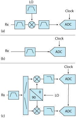
Figure 4 Common receiver architectures: superheterodyne (a) direct sampling (b) and direct conversion (c).
Three receiver architectures— superheterodyne, direct sampling and direct conversion—are the most commonly used in phased arrays (see Figure 4). Although only the receiver is shown, the topologies also apply to the waveform generator signal chains in the transmit path.
The superheterodyne approach, which has been around for 100 years, is proven and provides exceptional performance. Unfortunately, it is also the most complicated. It typically requires the most power and the largest physical footprint relative to the available bandwidth, and frequency planning can be quite challenging at large fractional bandwidths. The direct sampling approach has long been sought after, the obstacles being operating the converters at speeds commensurate with direct RF sampling and achieving large input bandwidth. Today, converters are available for direct sampling in higher Nyquist bands at both L- and S-Band. The technology is advancing, with C-Band sampling soon to be practical and X-Band to follow. Direct conversion provides the most efficient use of the data converter bandwidth. The data converters operate in the first Nyquist band, where performance is optimum and lowpass filtering is easier. The two data converters work together sampling I/Q signals, thus increasing the user bandwidth without the challenges of interleaving. The dominant challenge that has plagued the direct conversion architecture has been maintaining I/Q balance for acceptable levels of image rejection, LO leakage and DC offsets. In recent years, the advanced integration of the entire direct conversion signal chain, combined with digital calibration, has overcome these challenges, and the direct conversion architecture very practical in many systems. Table 1 summarizes the features of the three receiver architectures.
The industry is continually advancing the technology for all these signal chain options. The future will bring increased bandwidth and lower power, while maintaining high levels of performance, and integrated signal chains in system on chip (SoC) or system in package (SiP) solutions. Data converter analog performance will continue to improve, and these improvements will include increased sampling rates for wider bandwidth, increased channel count and maintaining the key performance metrics of noise density and linearity. These benefits will drive all of the RF signal chain solutions, enabling new phased array solutions. An area of increased importance at the system level is the recent addition of many digital functions that can offload FPGA processing and improve system capability (see Figure 5). Recently released data converters include digital down-conversion and filtering, potentially reducing the data rate to the FPGA, system power and FPGA processing requirements. Data converters will continue to add functionality, such as equalization and processing features at the front-end of digital beamforming.

HYBRID BEAMFORMING
At high frequencies or for low power systems, every-element digital beamforming is challenged by size and power requirements. The use of analog beamforming reduces the number of waveform generator and receiver channels required to be digitized. Analog beamforming is accomplished by adjusting the phase and amplitude of the signal at the individual antenna element to steer the direction of the radiation pattern. Figure 6a shows analog beamforming where independent phase shifters and attenuators are located in both transmit and receive signal paths, and the elements are combined in a single output. Figure 6b shows a functionally equivalent approach, where the phase shifter and attenuator are common, toggled between the transmit and receive paths at the antenna element. This latter topology reduces the number of phase shifters and attenuators but may require more frequent command updates to control the devices. To overcome the constraints of a single subarray, multiple subarrays can be used, with a topology as shown in Figure 7. In this approach, the outputs of the low noise amplifiers (LNA) at each element are split to feed many analog beamformers, where N elements produce M analog subarray beams. Each analog beamformer is programmed for a different antenna pattern. By repeating this topology across an array, digitally beamformed patterns can be created at widely disparate angles. This is one type of hybrid architecture that can provide the benefits of an every-element digital system with a reduced waveform generator and receiver count. The trade-off is the complexity of the analog beamformer.

Figure 5 Embedded digital features can offload the FPGA.
FRONT-END MODULES
Traditional analog beamformers have required a single-function GaAs phase shifter and single-function GaAs attenuator for each antenna element. More advanced approaches integrate the phase shifter and attenuator into a single GaAs MMIC that may include the power amplifier (PA), LNA and switch. SiGe BiCMOS technology can also realize the analog beamformer, even integrating four channels into a single IC, with the benefit of reduced footprint and lower power dissipation.

Figure 6 Approaches to analog beamforming: individual transmit and receive phase and amplitude control (a) and shared phase and amplitude control (b) for each element.
As the front-end or T/R modules provide the interface to the antenna element, the transmit power and efficiency and receive noise figure are critical requirements, set by the PA and LNA. Many systems also require provisions for calibration or additional filters. A functional block diagram of a front-end module containing the PA, LNA, and switch is shown in Figure 8. Many single function components are available that can be integrated into a single module. Custom ICs in various technologies support optimization and integration to meet the needs of the required application. Advances in GaN technology have created more efficient PAs with increased power density in the transmitter. GaN also enhances the receiver by providing LNAs with higher survivability to input power, eliminating the need for a discrete limiter. Higher levels of integration in both the beamformer and T/R module allow for flat-panel or tile arrays that are smaller and more cost effective to manufacture than other solutions, such as traditional plank or slat arrays or travelling wave tube (TWT) solutions.

Figure 7 Hybrid array architecture using M subarrays with analog beamforming to create N antenna beams.

Figure 8 T/R module integrating the PA, LNA and switch.
Conclusion
Digital beamforming phased arrays are becoming increasingly common, with rapid development expected to cover a wide range of applications and frequencies from L- through W-Band. The semiconductor industry is enabling new system developments with high speed converters, SiGe beamformers, microwave frequency conversion and front-end modules.