Broadband High Frequency SMT Packages
Kyocera America Inc.
San Diego, CA
For many years, the electronics industry has been using surface-mount technology (SMT) components because of their ease of integration, low cost and standardization. One drawback has been the lack of a single broadband, low parasitic package to fit the many higher frequency (above 6 GHz) applications. This need in the growing RF and microwave markets has provided motivation for the development of high performance packages with standard outlines and wide bandwidths. As a result, a family of SMT packages has been introduced for high frequency, broadband applications.
Recent Design Capabilities
With the recent advances in electromagnetic simulation and affordable computing power, many package design iterations can be performed quickly and structures that do not make the grade can be eliminated within hours instead of weeks. Utilizing these processes, several designs can be optimized before construction, saving time and materials. In addition, with commercial software, the basic equivalent circuit of the package transitions can be created and then optimized for higher frequencies. As a result, it has been demonstrated that packages that perform at frequencies up to 18 GHz with a surface-mountable structure are possible for wideband applications. Several unique package geometries (including air gaps, cutaway walls, slot vias and extra shadow layers of dielectric) have been modeled and produced. The unsuccessful variations were eliminated either for producability and/or performance drawbacks.
The Technical Approach
In the past, high frequency structure simulator software programs were used to simulate current package styles. These simulations were used as a base line and, as improvements were made, prototypes were built and measured. This procedure was not performed as a single study, but as an evolution of several projects with the intent of producing a reliable discrete package and optimizing the via transitions.
The modeling initially was performed on a one-quarter section of the whole package. The transmission line (lead) was mirrored about the axis of electrical symmetry with a 50 W impedance line on a Duroid-type substrate and a ribbon bond while the second port was placed at what would be the center of the package. The structures that produced the most promising results were then expanded into more complete models to achieve results closer to the measurements of an actual package.
Figures 1 and 2 show the critical dimensions of the model, including the bottom substrate thickness T1, lead pad width W1, ground isolation width W2, pad-to-ground distance C1, pad-to-wall distance C2 and second-layer thickness C3. Although other dimensions were varied and simulated (even to the extent of building unique geometries such as slot vias and thinner metal wall thicknesses), the relatively simple parameters shown are enough to affect SWR performance considerably and maintain stable and repeatable package manufacturing.
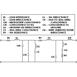
The initial equivalent circuit for this transition (simplified to some degree), shown in Figure 3 , is fairly complex. After several modeling and measuring iterations, T1, W2 and C3 were shown to be  dominant in minimizing parasitic capacitance and inductance. In fact, the historic standard package models did not include C3, a feature that was discovered with simulations. These dimensions were then optimized not only for electrical concerns, but for producability of the package as well.
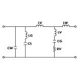
The results of the modeling and measurements produced a final geometry with the C3 layer as a dominant factor. Before the simulation the seal ring area was  considered small enough to be ignored where, in fact, it was later determined to be a source of reflection. Another dimension that was optimized was the distance from the signal via to the ground via. The results produced the simplified model shown in Figure 4 .
The Final Configuration
The resulting improvement in the SMT package return loss is shown in Figure 5 . Traditional cofired alumina processes and assembly techniques were utilized to keep the package hermetic and the properties of the materials known and predictable. The resulting packages exhibit remarkably flat return loss behavior up to K-band frequencies by optimizing the geometries and taking advantage of laminated ceramic processes and capabilities.
The new packages are commercially available and operate to 18 GHz with a broadband response. The packages are constructed from a 92 percent cofired alumina base, and Kovar seal ring (which improves isolation) and lead frame. The packages are completely hermetic (1 x 10⁸ atm cc/s) and pass Mil Standard 883 functional tests, including lead fatigue.
Standard open-tooled sizes are available and the package outlines permit automated processing. Custom designs and in-house measurements also are available.
Kyocera America Inc.,
San Diego, CA
(619) 576-2600.
