
Figure 1 Generalized two-port network.
Scattering parameters (S-parameters) were first mentioned in articles and textbooks in the 1950s and 1960s by Matthews, Collins and Kurokawa and popularized by the release of Hewlett Packard’s first network analyzers in the 1960s. Since then, S-parameters have been used to describe the complex characteristics of a network by quantifying the RF power flowing between its ports. S-parameters are essentially the ratio of the reflected and transmitted signal at a given port to the incident signal at a given port under perfect match conditions (see Figure 1). When referring to a transistor, these parameters can be used to calculate return loss, gain and isolation.1
It is important to understand that S-parameters are only truly valid for linear networks, where the characteristics of the network are independent of the level of the signal being driven into the network. When considering a semiconductor application such as a transistor, this refers to its small-signal operating condition, in which the input drive power does not affect the S-parameters of the transistor. Under small-signal operating conditions, a transistor will have linear gain at the fundamental drive frequency and not excite additional powers at the harmonic frequencies. Linear operation of a transistor and the associated input and output waveforms are shown in Figure 2.
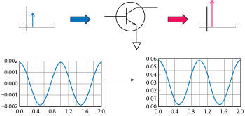
Figure 2 Linear operation of a transistor.
The question arises how to thoroughly describe and model a transistor operating under nonlinear large-signal conditions. These conditions occur commonly for high power and high efficiency power amplifiers operating in advanced classes of operation. Under these operating conditions, powers are induced at harmonic frequencies when excited by a sine wave, and in-band and out-of-band modulation products are created under modulation excitation. Considering a simple sine wave excitation, a transistor’s characteristics are dependent on the level of the input drive signal, shown in both frequency and time domains in Figure 3.
When the transistor is in deep compression and its output is composed of multiple harmonics, the device behavior cannot be described correctly by S-parameters, which are frequency domain quantities. It is much more natural to analyze the behavior of the device under test (DUT) in terms of time domain RF voltage and current waveforms. Clear evidence of this is provided by the theoretical description of the different modes of operation of power amplifiers, which is completely done in time domain. In this case, a nonlinear vector network analyzer (NVNA) can be used to measure the incident and reflected a- and b-waves at the transistor input and output, in both amplitude and phase. The data can then reconstruct the time domain RF voltage and current waveforms and RF load lines as well as all the conventional performance parameters of the device, such as input and output power, gain and efficiency.2

Figure 3 Nonlinear operation of a transistor.
Several commercial solutions exist to measure nonlinear transistor performance. This article will compare Maury Microwave’s MT4463 large signal network analyzer (LSNA) and the MT2000 mixed-signal active load-pull system (MSALP). The MT4463 LSNA was offered in conjunction with Agilent’s Network Measurement and Description Group between 2003 and 2008. The MT2000 is currently offered as an integrated non-50 Ω measurement system, in conjunction with Anteverta-mw.
MT4463 Large Signal Network Analyzer
The LSNA concept was first introduced in the 1980s by researchers using oscilloscopes to measure voltage and current waveforms at the gate and drain of a transistor. Research continued through the late 1980s and early 1990s with the goal of improving the capabilities of the technique. The breakthrough that led to the commercialization of the LSNA product occurred in 1994 with the release of the Hewlett Packard (HP) microwave transition analyzer (MTA). In 1996, HP designed the nonlinear network measurement system (NNMS), the precursor to the first LSNA, which was commercialized in 2003 by Maury Microwave.
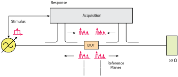
Figure 4 Signal flow of LSNA with exemplary 50 ohm termination.
The goal of the LSNA is to measure the wideband incident and reflected waves of a DUT at fundamental and harmonic frequencies using a periodic CW or periodically modulated signal, as shown in Figure 4. The injection signal is external to the core measurement instruments and, depending on the model selected, can be used to synthesize single-tone CW, pulsed CW or periodically modulated signals (i.e., multi-tone).
The hardware architecture of the LSNA is shown in Figure 5. The DUT has an associated input and output signal which can be represented by waves. The LSNA test set separates the incident and reflected waves into four measurement channels. A harmonic-sampler coherently down-converts the carrier and the harmonic and modulation frequencies to IF. A 14-bit digitizer and digital signal processor provides the raw signal data, and a computer performs error correction to represent the incident and reflected waves in the reference plane at the DUT. Additional software can plot the data in multiple formats (A/B, V/I, time, frequency or envelope).

Figure 5 Functional block diagram of the LSNA.

Figure 6 LSNA sampling converter.
The enabling technology of the LSNA lies in the HP MTA and its sampler-based technology, or sampling converter, as shown in Figure 6. With a sampler, all frequencies are acquired in the same measurement using a fixed LO, including the fundamental, harmonics, modulation and intermodulation frequencies.
In the default configuration, the LSNA is terminated with 50 Ω. Non-50 Ω measurements are enabled with the addition of passive or active tuners. Referring to Figure 1, the reflection coefficient ΓL presented to the DUT is the ratio a2⁄b2, where a2 is the “reflected” wave and b2 is the DUT’s transmitted power. In order to tune the impedance presented to a DUT, the signal a2 must be manipulated such that ΓL = a2⁄b2 is solved.
Passive mechanical tuners may be used to vary the impedance presented to the DUT. A passive slide-screw tuner (see Figure 7) consists of a precision 50 Ω slab line, with two parallel plates and a center conductor, and a metallic probe (or slug). When the probe is completely withdrawn from the slab line, the signal entering the tuner passes through with minimal interference, resulting in a low a2 signal. As the probe is lowered into the slab line, the electric field of the signal is interrupted, part of the signal is reflected back towards the DUT, and the a2 signal increases. As the probe’s horizontal position changes, the distance between the tuning element (probe) and the DUT changes, changing the phase of the reflection. By moving the probe up and down, left and right, nearly any impedance can be presented to the DUT, represented by full coverage of the Smith Chart (see Figure 8).
With open loop active load-pull, instead of using a passive tuner to reflect the signal back towards the DUT to manipulate a2, the signal is terminated, and a new signal a2 is introduced back towards the DUT. In this manner, the magnitude of reflection can be as large as the new a2 signal allows – even outside the Smith Chart – and created at the fundamental and harmonic frequencies.

Figure 7 Cross section and side view of the tuner, slab line and probe.
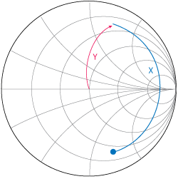
Figure 8 Impedance change by varying the horizontal (X) and vertical (Y) probe position.
One advantage of sampler-based measurements is speed, since the signal across the entire frequency spectrum is captured at once. Another advantage is signal type, since any periodic signal can be sampled. A disadvantage of sampler-based measurements is dynamic range, which is typically limited to approximately 60 to 70 dBc. The LSNA has been designed as a network analyzer using wideband receivers to measure vector corrected incident and reflected waves, allowing different types of external stimuli, including tuners, to be configured depending on the application. Therefore, external synthesizers are needed to create the injection signals to complete the network analyzer architecture. Also, any non-50 Ω analysis requires additional tuning networks, such as passive or active tuners. Passive tuners can be used with any injected signal, however they provide a wideband response which can distort wideband signals and degrade measurement results. Open loop active load-pull can be used with CW or pulsed-CW signals only.
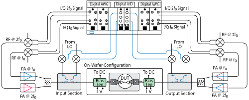
Figure 9 Functional block diagram of the MT2000.
The MT4463 LSNA covered two frequency ranges, 0.6 to 20 GHz or 0.6 to 50 GHz. The IF bandwidth was 10 MHz, RF frequency resolution was 1 kHz and the measurement dynamic range was 60 to 70 dB.3 Additional signal sources were necessary for multi tone or modulated signal synthesis, and passive or active tuners were needed for load-pull measurements.

Figure 10 Realistic wideband signal.
MT2000 Mixed-Signal Active Load-Pull System
The MT2000 MSALP is a NVNA with integrated wideband sources (two, four or six) that is capable of measuring a- and b-vector waves and S-parameters and with inherent wideband impedance control capabilities. The MT2000 covers between 300 MHz and 40 GHz, with 2, 4 or 6 active tuning loops, modulation bandwidths up to 240 MHz and a measurement dynamic range of 80 dB.4

Figure 11 Signal flow of the original injected signal, reflected signal and amplified signal.
The hardware architecture of the system is shown in Figure 9. Wideband arbitrary waveform generators (AWG) are used to create a wideband signal around baseband, which is then up-converted in the RF test set. The RF test set consists of local oscillators (LO) combined with I/Q mixers to up-convert the baseband signal to the fundamental and harmonic RF frequencies and inject source and load I/Q signals into the DUT. The resulting RF signal output is then down-converted back to baseband, and its a- and b-waves are analyzed by wideband analog-to-digital converters (ADC). Because both the AWGs and ADCs are wideband, a signal with up to 240 MHz of bandwidth can be generated and analyzed.

Figure 12 Signal flow of the original injected signal, reflected signal and amplified signal (black) and the generated signals for active tuning (red).

Figure 13 Time slotting of a CW signal for fast load-pull measurements.
To generate a wideband signal, a repetitive time domain modulated signal, compliant with industry standards, is generated and then analyzed in the frequency domain. The signal is composed of thousands of tones, as shown in Figure 10. The wideband signal is up-converted and injected into the DUT as a1. The resulting output signal b2 consists of a modified version of the original signal, including an amplified signal at the fundamental frequency (with the possibility of signal distortion if modulated) and signals at the harmonic and baseband frequencies. Because the device may not be physically matched at the input, part of the signal may be reflected as b1. The signal flow is shown in Figure 11.
Wideband impedance load-pull (see Figure 12) is achieved by varying a2 at Hz tone spacing to satisfy ΓL = a2 ⁄ b2 throughout the wideband signal. The wideband AWGs are used to create the pre-distorted CW, pulsed CW or modulated a2 signal at baseband, so the up-converted signal fulfills the desired wideband impedance grid at the fundamental and harmonic frequencies. The same technique can be used on the input to adjust the source impedances presented wideband at the fundamental and harmonic frequencies.
The wideband signal generation and analysis can also be used with single tone signals where the signal is divided in time. The record containing the wave modulation for a single modulated impedance can contain several wave magnitudes and phases representing many single tone impedances. Figure 13 shows an example of time slotting. In this manner, it is possible to load-pull 1000 impedance/power states per minute.
Conclusion
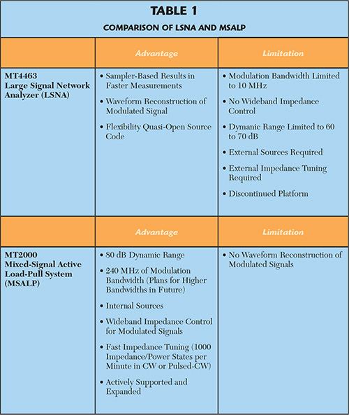
NVNA is a powerful tool to investigate, characterize and model transistor technologies operating under nonlinear conditions. Several commercial solutions offer NVNA capabilities, built around sampler or mixer technologies and each with their own advantages and limitations. A comparison of the two NVNA methodologies discussed in this article is in Table 1. In determining which approach to use, consider the type of injection signal required (CW, pulsed CW, single-tone, multi-tone or modulated), the level of measurement dynamic range, measurement speed, impedance control methodology (passive, narrowband active or wideband active), impedance control speed and system availability and support. It is clear that as measurement and signal-processing technologies evolve, newer solutions are overcoming the limitations of the past.
References
- D. M. Pozar, “Microwave Engineering,” John Wiley, New York, 2005.
- J. Verspecht, “Large Signal Network Analysis – Going Beyond S-Parameters,” ARFTG Microwave Measurement Conference short course notes, 2003.
- Maury Microwave, Data Sheet 4T-090, MT4463 Large Signal Network Analyzer (LSNA).
- Maury Microwave, Data Sheet 4T-095, MT2000 Mixed Signal Active Load Pull system (MSALP).
