High Isolation Switches with Integral Drivers
Mini-Circuits
Brooklyn, NY
Solid-state switches are used extensively for routing or selecting RF and microwave signals. If the isolation between the selected and unselected ports is not high, leakage of unwanted signals could degrade the carrier-to-interference ratio. Several switches may have to be cascaded to minimize this degradation and obtain the desired isolation. This cascaded configuration not only complicates the layout, but also increases the required PCB area. If the driver is an integral part of the switch, the task of cascading becomes even more complex. This article describes a new class of low cost, GaAs, high isolation SPDT switches with integrated drivers that can help solve this isolation problem.
The Mechanical Package
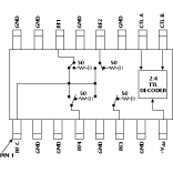
The switches’ packaging is a key element in achieving high isolation. The MMIC switch die is housed in a surface-mountable air cavity plastic package with 20  leads (16 gull-wing-style formed leads and four diagonal ground leads). In addition, the entire bottom of the package is grounded to provide additional shielding and low resistance from the active pins to ground. This configuration is essential for obtaining high isolation. At least two ground leads have been provided between the active pins to minimize crosstalk between the RF ports. Figure 1 shows the switches’ package outline and pin connection diagram.
The switch leads are solder plated and can withstand solder temperatures of up to 260°C. The package lid is injection-molded plastic and has a maximum temperature rating of 260°C. Sn63/Pb37 solder with a melting temperature of 190°C is recommended for attaching the MMIC package. The package is qualified to pass the MIL-STD-883D, Method 1014 pressurized leak test.
The Test Board
The test board and fixture used for testing the switches’ electrical performance have been constructed carefully to ensure accurate measurements. The packaged device is solder mounted onto a microstrip board, which, in turn, is mounted on a test fixture. A good RF ground is required for proper operation and to ensure that the isolation performance of the switch is not degraded.
The substrate layout must have a substantial number of via holes around the package area to reduce parasitic inductance. The recommended via hole size is 20 mils and the vias must be closely spaced (less than 60 mils apart). In addition, the via holes must be in close proximity to the package ground leads, but they should not be located under a ground lead. (A lead located directly on top of a via hole will not solder to the board properly.) The board material is multilayer Arlon 1000 with a dielectric constant of 10 ±0.3. The board is 24 mils thick and both the RF and DC lines are 22 mils wide.
The test board utilizes three SMA female RF input and output connectors. Supply voltages of +5 and –5 V DC are required for operating bias. In addition, TTL logic control (0 and 5 V) is required to test different switch states at each port. The switch control logic is listed in Table 1 .
|
Table I | ||
|
TTL Control |
RFout1 |
RFout2 |
|
Low |
On |
Off |
|
High |
Off |
On |
Electrical Performance
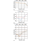
 The switches are available in reflective (ASW-2-50DR) and absorptive (model ASWA-2-50DR) versions and operate over the DC to 5 GHz frequency range. The units have a typical low insertion loss of 0.6 dB (1 dB maximum) from DC to 100 MHz, 0.7 dB (1.2 dB maximum) from 0.1 to 1 GHz, 1 dB (1.5 dB maximum) from 1 to 2 GHz and 1.6 dB (2 dB maximum) from 2 to 5 GHz. Figure 2 shows the switches’ measured insertion loss.
In addition, typical isolation is 70 dB (60 dB minimum) from DC to 100 MHz, 60 dB (50 dB minimum) from 0.1 to 1 GHz, 52 dB (47 dB minimum) from 1 to 2 GHz and 35 dB (28 dB minimum) from 2 to 5 GHz. The measured isolation is shown in Figure 3 .
The switches’ input return loss in the on state for the reflective switch and both on and off states for the absorptive switch is specified at 10 dB (min) from DC to 5 GHz and is typically 18 dB throughout that range. The absorptive switch contains a 50 W termination that is presented to the input in the off state. The internal load minimizes reflections from the output port. In the reflective switch, the output port is shorted to ground and is in a low impedance state. The choice 
 of configurations is largely dependent on the system demands. Figures 4 and 5 show the measured return losses for the reflective and absorptive switches, respectively. Output power at the 1 dB compression point is typically 25 dBm for both switch types at 1 GHz. Figure 6 shows the switches’ compression vs. power output at 1 GHz.
 Both switch versions feature integrated TTL driver circuits and have typical rise and fall times of 6 ns from 10 to 90 percent of the drive pulse. Switching speeds from 50 percent TTL to 50 percent RF are typically 7 to 14 ns. The switch driver control is TTL with the low level from 0 to 0.8 V and the high level from 2 to 5 V. The switches operate from ±5 V DC supply voltages, and typically draw 10 mA (20 mA maximum) current.
Conclusion
A new class of high isolation microwave TTL-driven, low cost switches has been introduced to reduce the effects of leakage signals contaminating system infrastructures. The use of these switches reduces the leakage of unwanted signals significantly and simplifies the overall system design and PCB layout. The prices of the switches are $19.95 for one to nine pieces and $14.95 for 10 to 49 pieces.
Mini-Circuits,
Brooklyn, NY
(718) 934-0003.
