
A Low Cost RF Transceiver for Data Communications
RF Micro Devices Inc.Greensboro, NC
Unlicensed radio devices in the European Community countries are expected to operate in compliance with standards proposed by the European Telecommunications Standards Institute (ETSI). Restrictions and regulations for operation of radio equipment in the 25 to 1000 MHz frequency band with transmit power levels up to 500 mW are contained in the Interim European Telecommunications Standard 300 220 (I-ETS 300 220) published by the ETSI. I-ETS 300 220 specifies performance standards for radios using all modulation types except code-division multiple access. I-ETS 300 220 distinguishes four main classes of radio equipment based on maximum output power and further distinguishes these devices as to whether or not the device operates inside or outside the industrial, scientific and medical (ISM) frequency bands. Of particular interest to battery-operated commercial wireless devices are the I-ETS 300 220 regulations and restrictions contained in Annex A related to operation of low power devices in the 433.050 to 434.790 MHz ISM frequency band. Annex A of I-ETS 300 220 includes the European Conference of Postal and Telecommunications (CEPT) administrations recommendation T/R 01-04, which has been adopted by the European Radiocommunications Committee. CEPT T/R 01-04 defines low power devices as radio devices that transmit a maximum effective radiated power (ERP) level of 10 mW or less. In general, the proposed restrictions for low power devices are much simpler than those that transmit higher RF power levels.  Basically, these restrictions allow for up to 10 mW ERP using any type of modulation. The maximum permissible out-of-band spurious and harmonic emissions are shown in Figure 1 . The flexibility and nonrestrictive nature of these regulations permit the development of a low cost data link for short-range communications.
The RF Transceiver
The model RF2906 IC was developed to serve as a low cost RF transceiver for data communications in the 433 MHz European ISM band. Integral to the RF2906 design process was the use of Optimum Technology Matching™ to select the appropriate IC technology for this application, meaning that all available RFIC technologies are considered for all new designs to develop the lowest cost solution that meets the technical requirements of a given application. The primary application for the RF2906 is in fixed wireless data links, such as those found in wireless security applications. In these applications, the end products are battery powered. As is the case with most battery-operated products, maximizing the product battery life is of primary importance. Since many low power transceivers might be employed in an application such as a wireless security system, the cost pressures on the components used in these products are extreme in order to make the system affordable for commercial or consumer customers. In the case of the RF2906, a 15 GHz silicon bipolar process technology was deemed an optimum technology match for this application. The silicon bipolar process selected provides a minimum geometry device that exhibits a 15 GHz ft under 3 V and 0.5 mA DC operation. Of the GaAs and silicon IC processes considered, this process allowed the DC power consumption objective for the RF transceiver IC to be achieved while keeping the cost of the IC below $5 in volume.
Functionally, the RF2906 provides a monolithic superheterodyne receiver, biphase shift-keying (BPSK) transmitter, VCO and dual-modulus prescaler, as shown in Figure 2 .  On-chip receiver functions include an RF low noise amplifier (LNA)/mixer, limiting IF amplifier strip, received signal strength indicator (RSSI), balanced IF multiplier (demodulator) and data amplifier. On the transmit side, a BPSK modulator and a transmit amplifier with analog level control are provided. The on-chip VCO and prescaler are intended to be used in conjunction with a number of commercially available CMOS phase-locked loop (PLL) ICs in applications requiring the frequency agility provided by a single loop synthesizer. For fixed-frequency transmit (or receive) applications, a one-port surface acoustic wave (SAW) resonator can be employed in the VCO circuitry to provide a fixed-frequency carrier (or LO in the receiver). A major operating feature associated with the RF2906 is an inherent transmit/receive (T/R) switch, which allows the chip to interface to a 50 W antenna (or RF filter) through a single pin. This feature eliminates the need for an external T/R switch and simplifies greatly the process of interfacing the device to an antenna.
The RF2906 transceiver is designed to operate half duplex and has four basic operating modes: sleep, lock, receive and transmit. The sleep mode allows the transceiver to be turned off completely to reduce the device current consumption to much less than 1 mA. When the IC is in the lock mode, the VCO prescaler and LO buffer circuitry are enabled to allow the PLL to achieve lock prior to enabling the receive or transmit functions. This timing avoids the possibility of an inadvertent spurious emission during the interval when the PLL is locking. The receive and transmit modes are intended to be enabled once the PLL has achieved lock. Table 1 lists a performance summary for the RF2906.
|
Table 1 - Transceivers Specifications | ||||
|
Parameter |
Conditions |
Min |
Typ |
Max |
|
Carrier frequency range (MHz) |
|
100 |
433 |
600 |
|
TX data frequency (MHz) |
|
|
|
2 |
|
Power level (dBm) (max) |
|
|
+8.5 |
|
|
Power level range (dB) |
analog control |
25 |
|
|
|
Power control sensitivity (dB/V) |
ave. over 3 V control range |
|
10 |
|
|
RF output SWR |
50 ohm; 433.9 MHz |
|
1.5 |
2 |
|
Receiver noise figure (dB) |
|
|
10 |
|
|
RF-IF conversion gain (dB) |
|
|
20 |
|
|
RX sensitivity (dBm) (min) |
IF BW = 150 kHz fRF = 433.9 MHz S/N = 8 dB |
|
-101 |
|
|
RSSI output voltage (V) |
|
|
0.4 to 1.7 |
|
|
RSSI transfer slope (dB/V) |
|
|
21 |
|
|
Data output level (V) |
|
|
0.2 to Vcc -0.2 |
|
|
Current consumption (mA) |
TX state at +10 dBm |
|
32 |
|
|
|
TX state at 0 dBm |
|
14 |
|
|
|
RX state |
|
4.6 |
|
|
|
power down state |
|
1 |
|
|
|
lock state |
|
3 |
|
|
Logic ( k ohm) |
3 V CMOS compatible control input resistance |
25 |
|
|
|
Supply voltage (V DC) |
|
2.7 |
3.0 |
5.0 |
|
Operating temperature (°C) |
|
-40 |
|
+85 |
|
Package type |
|
|
28-lead QSOP |
|
|
|
|
|
|
|
|
|
|
|
|
|
|
|
|
|
|
|
THE IC RECEIVER 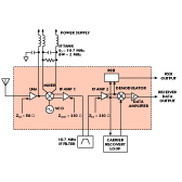
Figure 3 shows the IC’s receiver architecture. The main building blocks of the receiver are the LNA, RF mixer, IF amplifiers, demodulator and data amplifier. The receiver also utilizes the on-chip VCO.
Using temperature-compensated bias circuitry throughout the design, the RF2906 maintains nearly constant DC current consumption vs. temperature. In addition, on-chip line regulation is provided to minimize bias current variations due to supply fluctuations. Figure 4 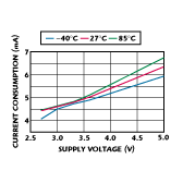 shows the measured DC current consumption of the IC in the receive mode over the supply voltage range of 2.7 to 5 V. By design, the temperature compensation of the bias current is optimized for 2.7 to 3.6 V applications.
The LNA/mixer cascade has a power gain of 20 dB and the receiver exhibits a cascaded single-sideband (SSB) noise figure (NF) of 10 dB. The RF front end consumes only 1.25 mA DC current to achieve this performance. In the receive or transmit mode, the RF input provides a 50 ohm input impedance. Although some sacrifice in receiver NF performance is made by incorporating the T/R switch on chip, the circuit architecture allows the transmitter and the receiver to share a common package pin. This feature offers space and cost savings by eliminating the need for an external T/R switch and any external matching circuitry.
An RF mixer architecture was selected that has an unbalanced RF input port in order to maintain DC current consumption at an absolute minimum, but the selected mixer consumes half the current of typical monolithic balanced mixers. Since the RF port is unbalanced, an external interstage bandpass filter is used between the LNA and mixer. This filter ensures that noise at the IF created in the LNA will be attenuated before reaching the mixer and, therefore, will not contribute to the overall receiver front-end NF. The RF mixer uses a single-ended input and downconverts to a balanced output. The input is a high impedance; the output impedance is fixed by the external components in the IF tank circuit, which consists of two inductors, a capacitor and a resistor that are tuned at the IF frequency. The inductors and capacitor are chosen for fo = 10.7 MHz and the resistor is used to fix the network bandwidth. This resistor also sets the output impedance of the mixer.
Once the signal is downconverted to the IF frequency, it continues to the IF portion of the chip. The IF section consists of the IF amplifiers, a RSSI, demodulator and data amplifier. The IF amplifiers are broken down into two separate stages. A pinout between the two IF stages is used for the IF filter. A ceramic 10.7 MHz IF filter is recommended, but filters for other IFs can be used if desired. This filter sets the bandwidth of the IF section, which is important for system-level calculations. The best sensitivity for the receiver will be achieved with the narrowest bandwidth filter that can be used while not degrading the signal that is being received.
A sample receiver sensitivity calculation for a system using the RF2906 is presented. The NF used is the SSB NF discussed previously, the bandwidth used is that of the IF filter and the IF signal-to-noise ratio (SNR) is chosen to be 8 dB. This SNR corresponds to a 10–4 probability of error in a BPSK system. The system designer must determine his or her own system requirements for bandwidth and SNR and modify the equation for that system. The 3 dB degradation due to the image noise is also taken into account. Using these specifications, the sample receiver sensitivity is expressed as
sensitivity = –174 + image noise
+ NF + 10logBW + SNR (dBm)
where
BW = noise-equivalent detection bandwidth
For the case where image noise = 3 dB and NF = 10 dB,
sensitivity = –174 + 3 + 10
+ 10logBW + SNR (dBm)
For example, if the system requirement is for an 8 dB SNR and an IF noise bandwidth of 150 kHz,
sensitivity = –174 + 3 + 10
+ 10log(150 kHz) + 8 (dBm)
= –101.2 (dBm)
To validate this calculation, a 433.9 MHz RF carrier BPSK modulated at a 1 kHz data rate (square wave) was input to the RF2906 receiver from a synthesized signal generator. Since the carrier recovery circuit is external to the device, the RF input, LO and injected IF carrier (to the demodulator) were input to the device from phase-locked signal generators to test the performance of the receiver alone. A 10.7 MHz ceramic filter with a 150 kHz, –3 dB bandwidth was used to set the IF bandwidth. 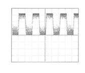 For an input level of –101.2 dBm, the recovered baseband data were observed using an oscilloscope, as shown in Figure 5 . Without a bit error rate tester, it is not possible to validate that the baseband output provides the desired 10–4 bit error rate, but the quality of the data output appears capable of being processed reliably.
The RSSI works with the IF amplifiers to provide a DC output voltage proportional to the strength of the RF input signal. 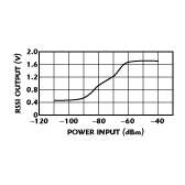 A graph of the RSSI response, shown in Figure 6 , displays a typical range of 0.4 to 1.7 V over an RF input power range of 50 dB. The RSSI on the RF2906 is intended for use as a signal presence indicator. When an RF signal is received, the RSSI output increases. This RSSI increase could be used to wake up circuitry (such as a microprocessor) that is normally in a sleep-mode configuration to conserve battery life. The RSSI could also be used in a simple AM on-off keyed (OOK) system as the demodulator. An external data amplifier would be necessary to convert the output to rail-to-rail data bits in this type of system. This configuration would require only an external operational amplifier and a few extra components.
Another application for which the RSSI could be used is to determine if the transmit power may be reduced in a system. If the RSSI detects a strong signal, it could instruct the transmitter to use the level adjust feature to reduce the power transmitted to save current consumption. This configuration would require an intelligent system, but the battery savings may be significant for some applications.
The output of the IF amplifiers feeds a balanced mixer that is intended for use as a BPSK demodulator. One output of the IF strip is pinned out so that an external carrier recovery loop may be used to input a coherent carrier signal to the demodulator input for BPSK operation. This demodulator will also function as an FM demodulator by passing the signal across an FM discriminator or a quadrature tank circuit and then back into the demodulator.
The output of the demodulator is coupled internally to the data amplifier. This block is a one-bit analog-to-digital converter, which takes the demodulator output and amplifies it into a rail-to-rail data stream. This output expects a high impedance load of greater than 1 MW, which is compatible with CMOS inputs and allows the data amplifier to operate on minimal DC current.
The Transmitter and VCO/Prescaler
Due to the RF2906 transmitter’s versatility, the device is expected to be employed as a transmitter using a variety of data modulation techniques. Although the primary application of the transmitter is as a BPSK modulator, the transmitter also can be used as an OOK AM or FM data transmitter.  In addition, in applications that do not require the frequency agility afforded by a synthesized carrier, the RF2906 can be configured as a fixed-frequency transmitter by interfacing the on-chip VCO directly to a SAW one-port resonator. A block diagram of the RF2906, shown in Figure 7 , provides additional insight into how these transmit applications might be addressed.
The RF2906 provides a fully balanced positive feedback amplifier and an isolation buffer that compose the on-chip portion of the VCO. An external LC tuning network is required to establish the center frequency and tuning range of the VCO. Both the VCO and prescaler support operating frequencies in excess of 600 MHz. The VCO interface to the dual-modulus prescaler, transmit modulator and RF mixer is accomplished on chip. The VCO and 32/33 dual-modulus prescaler combination provide the additional functionality necessary to implement a PLL frequency synthesizer when used in conjunction with a CMOS PLL IC. The chip also includes an RF transmit amplifier with over 30 dB of analog level control. A fully balanced biphase modulator that operates at a data rate in excess of 2 Mbps is also included on chip. 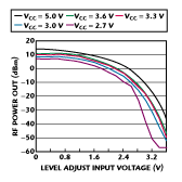
In order to appreciate how the RF2906 might be configured as an AM transmitter, Figure 8 shows a plot of the measured RF output power from the device as a function of DC input voltage on the level adjust pin for supply voltages in the range of 2.7 to 5 V. The level adjust input can be used to AM modulate (or OOK key) the carrier. Alternatively, the level adjust input can be used to reduce transmit power level while reducing DC power consumption simultaneously  in the transmit mode, as shown in Figure 9 . In OOK AM applications, the TX modulator maintains a good on/off ratio of greater than 30 dB over temperature and supply voltage. To demonstrate the performance of the RF2906 as an OOK AM transmitter, a logic level 200 kHz square wave was input to the level adjust pin and the RF output was observed using a digitizing oscilloscope. The 433 MHz OOK RF carrier and the data input waveforms measured are shown in Figure 10 .
In FM data applications, the modulation signal is applied to an external varactor used in the VCO circuit. If the modulation signal is much higher in frequency than the PLL loop bandwidth, the carrier frequency will vary in accordance with the modulation input. The FM deviation desired can be obtained through appropriate selection of the varactor and the amplitude of the modulation input.
For applications requiring a fixed-frequency transmitter, a SAW one-port resonator can be interfaced to the RF2906, as shown in Figure 11 .  This circuit can also be utilized in high data rate applications to mitigate the amount of incidental FM induced on the carrier, or simply as a means to reduce the number of parts used in the product design. Incidental FM can be an issue in BPSK applications where the modulation rate is higher than the PLL bandwidth. For modulation rates inside the PLL bandwidth, the PLL will suppress the incidental FM that is induced, making it much less of a concern. The amount of incidental FM suppression provided by the PLL will depend on the PLL bandwidth, modulation rate, excess loop gain at the modulation frequency and tuning sensitivity of the VCO. Using the high Q SAW device for frequency control, the incidental FM induced on the carrier was reduced significantly over the open-loop VCO characteristics. Using the SAW one-port resonator, the incidental FM observed on the carrier was less than ±5 kHz and was independent of modulation rate. An important consideration in spread spectrum BPSK applications is carrier suppression provided by the modulator. Using a 423.3 MHz one-port SAW resonator to provide a fixed-frequency LO and 500 kHz square wave (0 to 3 V) data input to the modulator, the carrier
  suppression of the modulator (at the transmitter output) was observed using a spectrum analyzer. The device achieved approximately 29 dB of suppression under these conditions, as shown in Figure 12 .
In a typical 433 MHz BPSK system based on the RF2906, a serial input frequency synthesizer is used with the RF2906’s prescaler and VCO. A digital application-specific IC (ASIC) processes the data from the RF2906 and controls the operational modes of the transceiver. The digital ASIC also sends the counter data to the PLL IC to fix the frequency of the synthesizer loop. An external carrier recovery loop provides the necessary input for the demodulator to process BPSK signals. 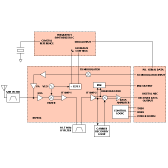 Figure 13 shows a detailed block diagram of the BPSK system. An external SAW filter used at the transmitter output is required to attenuate harmonics from the transmitter.
Conclusion
A low cost bipolar silicon IC has been developed that offers robust performance in wireless radio applications. The chip allows devices to be customized to meet specific requirements for a low power transceiver. The device operates over a supply voltage range of 2.7 to 5 V and can be configured for BPSK, amplitude-shift keying or FM data modulation. Price: less than $5 (in volume).
RF Micro Devices Inc., Greensboro, NC (910) 664-1233.