GaAs MESFET and Traveling Wave Tube (TWT) amplifiers have long addressed high power X-Band applications from 10 W to multi-kW. GaAs MESFET solid state amplifiers deployed range from 10 to 100 W while TWT deployment range extends power to multi-kW; these amplifiers have served applications such as satellite communications, marine radar, medical imaging and military.
0.4 micron GaN HEMT transistors were first released into the market during the 2005 to 2006 time frame. The initial GaN HEMT offering focused on UHF through C-Band, primarily on CW broadband power and L- and S-Band pulsed power applications. Since the initial release, GaN HEMT suppliers have successfully fielded several million transistors. At Cree, the reported field FIT rates are less than 10 parts per billion hours of device operation. This FIT value rivals or is superior to any GaAs or Si power FET technology demonstrating GaN HEMT has established itself as a reliable and accepted technology.
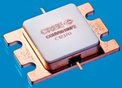
Recently, a 0.25 micron GaN HEMT process technology has been released and to date includes product in die form, foundry service and X-Band fully matched packaged transistors. The X-Band matched device product family consists of four products:
- CGHV96050F1: 50 W, 50 Ω matched transistor tested under OQPSK at 25 W Pave from 7.9 to 8.4 GHz
- CGHV96100F1: 100 W, 50 Ω matched transistor tested under OQPSK at 50 W Pave from 7.9 to 8.4 GHz
- CGHV96050F2: 50 W, 50 Ω matched transistor tested from 7.9 to 9.6 GHz under 100 µsec, 10 percent duty cycle
- CGHV96100F2: 100 W, 50 Ω matched transistors tested from 7.9 to 9.6 GHz under 100 µsec, 10 percent duty cycle

Figure 1 CGHV96050F1 typical performance spectral mask under OQPSK modulation, 1.6 Msps VDD = 40 V, output power = 44 dBm/25 W (a) and linear output power, gain and PAE, VDD = 40 V, IDQ = 500 mA, 1.6 Msps, OQPSK modulation at –30 dBc (b).

Figure 2 CGHV96100F1 typical performance spectral mask under OQPSK modulation, 1.6 Msps VDD = 40 V, output power = 47 dBm/50 W (a) and linear output power, gain and PAE, VDD = 40 V, IDQ = 1000 mA, 1.6 Msps, OQPSK modulation at –30 dBc (b).
The CGHV96050F1 and CGHV96100F1 are characterized for satellite communication linear power requirements under OQPSK. Figures 1 and2 show the linear features over frequency based on -30 dBc offset mask. Both the 50 and 100 W, X-Band GaN HEMT transistors show excellent linearity in the 30 percent power added efficiency (PAE) range while providing linear gain exceeding 12 dB. The spectral compliance is achieved while operating at 3 dB backed-off from Psat.

Figure 3 Intermodulation distortion performance vs. tone spacing, VDD = 40 V, frequency = 8.2 GHz, output power = 43 dBm/20 W.
The CGHV96050F1 and CGHV96100F1 can be deployed in 25 to 100 W linear power solid state amplifiers (SSPA) which have earlier typically utilized GaAs MESFET technology. Devices are easily combined. For example, a high power SSPA could be developed with multiple combined 100 W transistors. Typical performance for a four-way combined 100 W transistor could realize a 200 W average power linear amplifier. TWTs typically operate at 6 dB back-off from their saturated power and in many cases require external linearization to be able to meet the linearity requirements for satellite communications. A 200 W GaN HEMT linear performance (400 W peak power) would be equivalent to a corresponding 800 W TWTA in terms of linear power performance capability.
The CGHV96050F1 and CGHV96100F1 offer the wide video bandwidth capabilities important for multi-carrier satellite communication applications. Figure 3 shows tone spacing through 80 MHz separation while maintaining spectral stability in terms of IM3, IM5 and IM7.

Figure 4 CGHV96100F2: 100 W X-Band internally matched transistor (a) and CGHV96050F2: 50 W X-Band internally matched transistor (b) performance.

Figure 5 Output power vs. time, DD = 40 V, PIN = 41 dBm, duty cycle = 10%.
The CGHV96050F2 and CGHV96100F2 GaN HEMT transistors have also been characterized for saturated power, pulsed applications such as weather and marine radar as shown in Figure 4. The transistors offer a minimum power gain of 10 dB while offering 80 or 140 W output power over the 7.9 to 9.6 GHz frequency band and PAE offered is 45 to 50 percent. These features correspond to an average of two times improvement over comparable GaAs MESFET transistors at this frequency and power level.
The pulse droop demonstrated by the 50 and 100 W GaN HEMT transistors is excellent as shown in Figure 5. Short pulse width droop is extremely low and even a relatively long (for this application) 300 µsec pulse droop is a very good 0.5 dB as shown in the figure. The minimal pulse droop is due to the superior thermal properties of the Silicon Carbide (SiC) substrate used as a substrate material for the GaN-on-SiC HEMT structure.
These high power X-Band transistors offer excellent features for 50 thru 100 W requirements and can be combined into high power SSPAs exceeding 1 kW by deploying 100 W transistors into a multiple device combination scheme. The advantages of GaN HEMT transistors for X-Band will offer significant systems benefits in terms of power management, thermal management, power supply load, package size shrink of the SSPA unit size or offering significant reliability and cost advantages when compared with TWTA. GaN HEMT SSPA system advantages are overwhelming when compared with GaAs MESFET-based SSPA and TWTA.
Cree Inc.,
Durham, NC
(919) 407-7816,
www.cree.com/rf.
