Wideband, low noise, generic gain block and driver amplifier MMICs have been developed using many different device technologies including MESFET, HBT and PHEMT. Among these, PHEMT-based MMIC technologies have achieved superior performance due to inherent device high frequency operation capability. In order to achieve superior performance similar to PHEMT technologies, multifunction self-aligned gate (MSAG“)-based MMICs are implemented using a multi-level plating (MLP) process. MLP utilizes multiple low dielectric constant polyimide and thick metallization layers atop the base GaAs. Designing with MLP allows for lower loss transmission lines or matching networks,1–3 higher frequency operation and increased flexibility in the development of higher power components.
At the M/A-COM facility in Roanoke, VA, the MSAG MESFET process4–9 is being used to develop low cost, high volume, high performance and highly reliable multifunction monolithic ICs for commercial and military applications. Because of its versatility in integrating low noise, power and high speed large-scale integration (LSI) functions on a single chip, the process has been named the multifunction self-aligned gate process. The MSAG process eliminates the need for a gate recess, the single most important yield and reproducibility-limiting step. As each device type, which may include EFET, DFET, Schottky diode/limiter, low noise FET, switching FET, power FET and n' implants, is optimized for its respective function, it requires an additional mask. The MSAG process is available as a standard foundry service to outside users.
Multi-level Plating Process
Figures 1 and 2 show stylized cross-section views of standard and MLP-processed GaAs wafers. A common design rule, set for core structures and common GaAs processing techniques, except for the MLP-unique elements, allows for simplified design, layout and processing.

Fig. 1 Standard “Process 5” wafer cross-section.
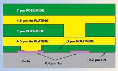
Fig. 2 Multi-level plating (MLP) process wafer cross-section.
There are two key differences between the standard and MLP-processed MMICs. The first is the addition of a second, 7 µm thick, low dielectric constant polyimide layer; the second difference is the addition of a second thick, 4.5 µm, gold metallization layer. These two additions provide the MLP advantages.
With the additional polyimide layer, a designer has the flexibility to locate transmission lines, known as multilayer microstrip lines, on polyimide up to 10 µm thick. The impedance of such lines can be increased by 40 to 60 percent — as compared to standard lines on the given base substrate. The high impedance capability of MLP is well suited for implementing low loss matching networks and improving the bandwidth of passive components.
The additional thick metallization layer offers benefits as well, mostly in the area of DC current routing/high power design and extending the usage of passive components to lower frequencies. Most straightforwardly, the designer now has the flexibility to use 9 µm thick transmission lines. Current handling for such lines is 20 mA/µm.
A second benefit of the additional thick metal layer is the option to create high current structures, such as spiral inductors. Previously, spiral inductors have been current limited, based on the width of the thin metallization underpass to access the center of the spiral, typically 2 mA/µm… as compared to 10 mA/µm for 4.5 µm thick lines. With MLP, a spiral inductor can be fabricated with 4.5 µm thick spirals and 4.5µm thick underpasses.
The configuration of the multilayer microstrip line is shown in Figure 3, where εr and εrd are the relative dielectric constants of the GaAs substrate and polyimide buffer layer, respectively, and h and d are their respective thicknesses. The thickness of the polyimide could be between 5 and 25 µm. However, the MLP process only allows polyimide thicknesses of 3, 7 and 10 µm. The microstrip conductor W has an approximate thickness of 4.5 µm. Typical dielectric constant values for GaAs and polyimide are 12.9 and 3.2, respectively. Measured results for the multilayer microstrip structure are summarized in Table 1. As an example of the reduced loss characteristics of MLP, on a bare 75 µm GaAs substrate, a 50 Ω line is about 50 µm wide, whereas with a 10 µm polyimide layer atop the base GaAs, it is approximately 90 µm wide. The losses are 0.83 and 0.41 dB/cm, respectively, a 50 percent reduction for the 50 Ω line on polyimide. Further improvement may be obtained by etching away the surrounding polyimide, so that more of the microstrip is surrounded by air. This configuration is also compatible with multi-level plating MMIC fabrication processes.

Fig. 3 Two modified microstrip line configurations.

A family of 6.7 nH inductors was also characterized, and their figure of merit indexes (FMI) is compared in Table 2. FMI is defined as

where
fres = self-resonance frequency

The inductors selected are a standard inductor with thin metal underpass, a MLP multilayer inductor with 9 µm thick spiral metallization and a 3-D inductor. The Q values are obtained at the maximum Q frequency. It is easily noted that the 3-D structure has the best FMI. This is because of its reduced area. A trade-off of this inductor type is that it has the lowest resonance frequency due to higher inter-level capacitances. The Q factor for the 3-D inductor is about 23 percent higher than for the standard inductor but about 16 percent lower than for the multilayer inductor using thick metallization. The FMI for the 3-D inductor is about 2.6 times larger than for the standard inductor.
A final example of the benefits of MLP is a broadband 3 dB coupler, which is required in many microwave applications. MLP is also suitable to realize tight directional couplers on GaAs substrates. A 3 dB asymmetric broadside coupler was developed using the MLP process on a 75 µm thick GaAs substrate. Figure 4 shows the top-sectional view of the broadband coupler, which operates over the 7 to 15 GHz frequency range. The physical length of the coupler is 3000 µm. The bottom and top conductor line widths are 40 and 60 µm, respectively, resulting in a lower dissipated loss than for a Lange coupler on GaAs. As shown in Figure 5, the measured insertion loss in the coupled and direct ports are 3.3 ± 0.5 dB and 3.5 ± 0.5 dB, respectively. The measured return loss was better than 18 dB.

Fig. 4 Physical layout of the 3 dB asymmetric broad side coupler.

Fig. 5 Measured performance of the 3 dB coupler.
The MLP process results in improved performance in MMIC passive components including couplers, filters, dividers/combiners and transformers, and also allows the realization of new MMIC components including thin film microstrip, multi-level inductors, tight couplers and baluns.
Distributed Amplifiers Using the MLP Process
At the circuit level, improvements in performance can be achieved using very high impedance lines (microstrip lines on 10 µm polyimide) in the gate and drain equivalent transmission lines of a distributed amplifier, using low loss matching networks at the output of a power amplifier, using high current carrying capacity inductors in matching networks and using 9 µm thick conductors instead of 4.5 µm thick conductors having twice the width. An approximate expression for the small-signal gain of a distributed amplifier is given by10

where
n = number of FETs
gm = transconductance per FET
Z0 = characteristic impedance of the gate line
αg = attenuation constant of the gate line
lg = length of gate line per unit cell
In this expression, a constant characteristic impedance and a constant unit line length have been assumed. Also, the drain line losses are neglected. Equation 2 shows that, for higher gain, one needs higher Z0 and lower αg. As previously shown, MLP provides both these features.
As an example of the performance benefit MLP provides for wideband MMICs, Figure 6 shows the predicted performance of a pair of 2 to 20 GHz distributed amplifiers, one designed using standard Process 5 techniques and the other implemented in MLP. As is easily noted, approximately 1.5 dB additional gain is provided by the MLP design at 20 GHz. Thus, MLP can be used to either increase gain for a given bandwidth, or provide additional bandwidth for a given amount of gain.

Fig. 6 Predicted performance of a 2 to 20 GHz distributed amplifier using a standard “Process 5” (dashed lines) and MLP (solid lines) processing.
In the following, examples of distributed amplifiers developed using MSAG FET with the MLP process are described. In these MMICs, the gate and drain microstrip conductors are on a 10 µm thick polyimide layer atop the GaAs substrate. The circuits were designed using small-signal models for the FET devices and matched to 50 Ω at the input and output.
2 to 20 GHz Distributed LNA (Self-biased)
Figure 7 shows the physical layout of a 2 to 20 GHz distributed LNA, incorporating six 150 µm 5N (low noise) FETs. The circuit was designed for low noise figure and high gain using a low noise FET model. A single supply operation is provided through the use of on-chip self-biasing networks. The value of the resistor between the source of the device and ground is selected to bias the device at 0.25 IDSS to provide a trade-off between minimum noise figure and high P1dB. The drain supply voltage is 5 V. The chip size is 3 × 1.6 µm.
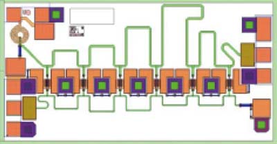
Fig. 7 Layout of a 2 to 20 GHz self-biased distributed LNA.
Figures 8 and 9 show the measured LNA gain and noise figure, and P1dB, respectively. The current under drive increases from 75 mA at the Q-point to about 110 mA at the P1dB compression point. The measured return loss was better than 10 dB over the 2 to 20 GHz frequency range.

Fig. 8 Measured gain and noise figure of self-biased 2 to 20 GHz distributed LNA.

Fig. 9 Measured P1dB of self-biased 2 to 20 GHz distributed LNA.
2 to 18 GHz Distributed Amplifier Driver (Self-biased)
Figure 10 shows the physical layout of a distributed driver amplifier (DA), designed for the 2 to 18 GHz frequency band. It is comprised of five 5N FETs, each having a 300 mm gate periphery. The circuit was designed for high P1dB and high gain while providing a good match to 50 Ω at the input and output. A single supply operation is provided through the use of on-chip self-biasing networks. The nominal drain supply voltage is 5 V; however, on-chip voltage drop resistors allow variable supply voltage from 5 to 8 V. The chip size is 3 × 1.7 mm. Figure 11 shows the measured gain and return loss; Figure 12 demonstrates the saturated power at different drain biases.

Fig. 10 A 2 to 18 GHz self-biased distributed driver amplifier.

Fig. 11 Small-signal gain, and input and output VSWR at VD = 5 V of the distributed amplifier driver.
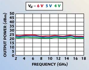
Fig. 12 Saturated output power of the distributed amplifier driver as a function of frequency and drain voltage.
2 to 18 GHz Distributed Power Amplifier
This is another DA, designed for higher power level. It uses the same approach as discussed previously. This topology employs five 300 µm 5A (power) FETs biased at 8 V. The physical layout of this circuit is shown in Figure 13. The MMIC is over-sized at 3.0 × 1.7 mm due to the limitations of being in a development mask. In a production mask, the final chip size would be 2.3 × 1.4 mm. Figures 14 and 15 show the measured gain and noise figure, and output P1dB, respectively.

Fig. 13 Layout of a 2 to 18 GHz distributed power amplifier.

Fig. 14 Measured gain and noise figure of the 2 to 18 GHz distributed power amplifier.

Fig. 15 Measured P1dB of the 2 to 18 GHz distributed power amplifier.
2 to 8 GHz Driver Amplifier
Another useful feature of MLP is to create high current inductors for broadband and compact designs.11 In this section, a broadband 0.7 W driver amplifier developed using MLP inductors is discussed.
Traditionally, a driver amplifier is designed based on the loadline method.12–15 The design of the two-stage broadband MMIC driver amplifier was based on a design methodology using small-signal, nonlinear FET models and loadpull data obtained at the operating bias point. The operating point of the amplifier was selected for class-AB operation (0.30 IDSS) of the device in order to obtain the best compromise of power output, gain, PAE, linearity and variable power supply operation over the 2 to 8 GHz frequency range.
In this design, the loadline technique is used initially to optimize the circuit parameters. The optimum load impedances ZL1 and ZL2 at the drain of the first and second stage FETs, necessary to realize the maximum output power and PAE, are shown in Figure 16. Then, the design is simulated using the nonlinear model to calculate the power compression of each stage and the output power and PAE as a function of input power. Since it is very difficult to optimize the matching networks to the required load impedances over wide bandwidths, using nonlinear models, the above design process is repeated so that an optimum solution for simultaneous match to the load impedances at the drain of each FET and best gain, power and PAE are achieved.
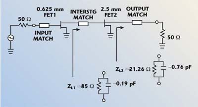
Fig. 16 Schematic of a two-stage driver amplifier.
The input stage, which has a limited gain compensation network, was designed for good input match as well as for maximum power transfer at the high frequency end. The interstage matching network was designed to provide a flat gain response and deliver enough power to the output stage FETs for achieving overall maximum output power and PAE. The output matching elements were selected to provide an optimum load match with minimum insertion loss, since efficiency and output power are reduced to a great extent by a passive loss. Both stages, as well as the complete amplifier, were designed to be unconditionally stable over 3 to 10 V drain power supply voltage and 0.25 to 0.50 Idss drain current. Experience has shown that for MSAG FETs, standard even-mode (K > 1) and odd-mode stability analyses are adequate to avoid microwave oscillations. However, under large-signal condition and pulsed operation, it is necessary to use worst-case K-factors greater than 1 when S-parameter data is used for various bias conditions from Vds = 3V, 0.50 Idss to Vds = 10V, 0.25 Idss. This approximately replicates the envelope a full cycle of the input signal experiences during the large signal and pulsed operation. It was found that imposing a K > 2.0 condition, for Vds = 10V and 0.25 Idss small-signal S-parameters, is about what is necessary to ensure K > 1 under all conditions.
Figure 17 shows the photograph of the two-stage 0.7 W power output driver amplifier. The chip size is 3 × 2 mm.

Fig. 17 A 2 to 8 GHz, 0.7 W driver amplifier.
Typical CW measured Pout and PAE for MMIC chips on Cu-W carriers at VDS = 8V and Pin = 18 dBm are shown in Figure 18. The amplifier has greater than 28.5 dBm power output and better than 24 percent PAE over the 2 to 8 GHz frequency range. Figure 19 depicts P1dB power levels at various drain voltages. The variations of small-signal gain and input VSWR as a function of frequency are shown in Figure 20. The input VSWR is better than 2:1 over the 1.5 to 8.4 GHz range.

Fig. 18 Pout and PAE of the 2 to 8 GHz driver amplifier at VD = 8 V PIN = 18 dBm.
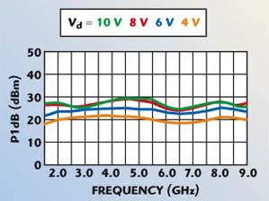
Fig. 19 P1dB of the 2 to 8 GHz driver amplifier as a function of drain voltage.

Fig. 20 Small-signal gain and input VSWR of the 2 to 8 GHz driver amplifier at VD = 8 V.
Conclusion
A family of wideband, low noise, generic gain block and driver amplifier MMICs for commercial and military applications has been developed. Using MLP processing, higher performance and higher frequency operation are achieved.
Acknowledgment
The authors wish to acknowledge the support of ADBU layout and test groups and the MSBU wafer-processing group in the successful development of the above MMICs.
References
- I.J. Bahl, et al., “Low Loss Multilayer Microstrip Line for Monolithic Microwave Integrated Circuits Applications,” International Journal of RF and Microwave Computer-aided Engineering, Vol. 8, November 1998, pp. 441–454.
- I.J. Bahl, “High Current Capacity Multilayer Inductors for RF and Microwave Circuits,” International Journal of RF and Microwave Computer-aided Engineering, Vol. 10, March 2000, pp. 139–146.
- I.J. Bahl, “High Q and Low Loss Matching Network Elements for RF and Microwave Circuits,” IEEE Microwave Magazine, Vol. 1, September 2000, pp. 64–73.
- A.E. Geissberger, R.A. Sadler, M.L. Balzan and J.W. Crites, “TiW Nitride Thermally Stable Schottky Contacts to GaAs: Characterization and Applications to SAG FET Fabrication,” Journal of Vacuum Science and Technology, Vol. B5, 1987.
- A.E. Geissberger, R.A. Sadler, E.L. Griffin, I.J. Bahl and M.L. Balzan, “Refractory Self-aligned Gate Technology for GaAs Microwave FETs and MMICs,” IEEE Transactions on Electron Devices, Vol. 35, No. 5, May 1988, pp. 615–622.
- A.E. Geissberger, I.J. Bahl, E.L. Griffin and R.A. Sadler, “A New Refractory Self-aligned Gate Technology for GaAs Microwave Power FETs and MMICs,” IEEE Transactions on Electron Devices, Vol. 35, No. 5, May 1988, pp. 615–622.
- A.E. Geissberger, et al., “Fabrication, RF Performance and Yield of a Combined Limiting Amplifier and Dual-modulus Prescaler GaAs IC Chip,” IEEE Transactions on Microwave Theory and Techniques, Vol. 36, No. 12, December 1988, pp. 1706–1713.
- I.J. Bahl, et al., “Multifunction SAG Process for High Yield, Low Cost GaAs Microwave Integrated Circuits,” IEEE Transactions on Microwave Theory and Techniques, Vol. 38, No. 9, September 1990, pp. 1175–1182.
- W.L. Pribble and E.L. Griffin, “An Ion-implanted 13 Watt C-band MMIC with 60% Peak Power Added Efficiency,” IEEE Microwave and Millimeter-wave Monolithic Circuits Symposium Digest, 1996, pp. 25–28.
- Y. Ayasli, et al., “A Monolithic GaAs 1–13 GHz Traveling-wave Amplifier,” IEEE Transactions on Microwave Theory and Techniques, Vol. 30, No. 7, July 1982, pp. 976–981.
- I. Bahl, Lumped Elements for RF and Microwave Circuits, Artech House Inc., Norwood, MA, 2003.
- S.C. Cripps, RF Power Amplifiers for Wireless Communications, Artech House Inc., Norwood, MA, 1999.
- E.L. Griffin, “Application of Loadline Simulation to Microwave High Power Amplifiers,” IEEE Microwave Magazine, Vol. 1, June 2000, pp. 58–66.
- K. Chang, I. Bahl and V. Nair, RF and Microwave Circuit and Component Design for Wireless Systems, John Wiley & Sons Inc., Hoboken, NJ, 2002, Chapter 11.
- I. Bahl and P. Bhartia, Microwave Solid State Circuit Design, Second Edition, John Wiley & Sons Inc., Hoboken, NJ, 2003, Chapter 10.
