This article describes a 2 GHz CMOS complementary voltage-controlled oscillator (VCO) with differentially tuned MOS varactors for ISM-band wireless communications applications. The VCO is fabricated using a 0.25 µm mixed-signal/RF CMOS process. This VCO, utilizing differentially tuned MOS varactors, can reduce the adverse effect of high varactor sensitivity by rejecting the common-mode noise. The measurements listed in Table 1 are performed using an FR-4 PCB test fixture. The output power of the VCO is 8.2 dBm with a power consumption of 8 mA at VDD = 2.5 V, excluding buffer amplifiers. The output frequency of the VCO varies from 1827 to 2136 MHz with a 309 MHz or 16 percent tuning range and its phase noise is –100.2 dBc/Hz at a 100 kHz offset.

For a mixed-signal and system on a chip (SoC) design, it is very important to reduce the effect of the common-mode noise coupled through the substrate. In general, differential circuits are preferred, in a single chip radio, to minimize the effects of common-mode noise from other circuits such as digital and analog baseband blocks. For the same reason, LC tank, voltage-controlled oscillators (LC-VCO) of inherent differential structures have been widely used to design a VCO with a low phase noise. However, though the LC-VCO circuit has differential outputs, it does not have a differential control input. If the noise signals are coupled to the control input signal, the phase noise or jitter will be significantly degraded by the AM-to-PM conversion process. Therefore, a fully differential LC-VCO must not only have differential outputs, but also differential control voltage inputs. Its implementation is an important issue. As feature sizes are scaled down to deep sub-micrometer in modern CMOS process technology, a very thin gate oxide is required to maintain short-channel effects at an acceptable level. This leads to a low breakdown voltage of the device and, therefore, the supply voltage has to decrease proportionally. The lowering of the supply voltage, due to technology scaling, decreases the frequency tuning range. For example, the supply voltage drops from 3.3 to 2.5 V for a change in technology from 0.35 to 0.25 µm. The range of the varactor control voltage decreases accordingly, resulting in reduced frequency tuning range if the varactor gain remains the same. Therefore, for low voltage CMOS, a higher sensitivity varactor is required for the VCO to achieve a respectable performance. However, high varactor sensitivity is unfavorable to phase noise performance, as described by the modified Leeson’s formula.1 A band-switching topology can be employed to reduce the effect of varactor sensitivity while maintaining the required frequency tuning range,2 but extra control circuitry is required for switching the varactors, which complicates the phase-locked loop (PLL) locking procedure. This article presents another method: differential tuning of the MOS varactors3 to avoid the drawbacks of the effect of high sensitivity.

Circuit Design
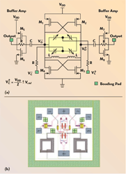
Figure 1 shows a 2.4 GHz CMOS transceiver RF front-end, which uses a single mixer transceiver architecture for ISM-band wireless applications. A 2 GHz VCO designed for this CMOS transceiver is shown in Figure 2. The VCO is fabricated with a 0.25 µm mixed-signal/RF CMOS process. The core circuit of the 2 GHz VCO is a complementary cross-coupled pair with both PMOS and NMOS, which generate a negative resistance to compensate for the losses in the LC resonator. There are several reasons for the advantage of the complementary structure used as the core circuit of the VCO. The complementary structure offers a higher transconductance for a given current, which results in faster switching of the cross-coupled differential pair. It also offers better rise- and fall-time symmetry, which results in less up-conversion of 1/f noise and other low frequency noise sources.4 For the devices used in this oscillator, a minimum channel length of 0.25 µm is used and the appropriate channel widths are chosen to make the transconductance of NMOS equal to the transconductance of PMOS. Therefore, the DC level of the drain nodes in the complementary cross-coupled pair can be maintained as VDD/2 in order to achieve a more symmetric waveform. The voltage source of M1, M2, M3 and M4 is directly connected to 0 V and VDD (2.5 V), respectively, without any extra current source. For low supply voltage operation, enlarging the voltage swing by removing the use of a current source, which reduces the voltage headroom, is one of the most direct ways to improve the phase noise performance. This bias scheme maximizes the oscillator signal peak-to-peak amplitude. The series combination of the two on-chip inductors constitutes the tank inductor. Because the layout of the inductor is asymmetric, two inductors in series, placed in a vertically symmetric way, ensure that the same structure could be seen by the drain nodes of the cross-coupled pair. This will result in a more symmetric waveform between the two drain nodes. In this design, one side of the MOS varactor is connected directly to the drain node of the cross-coupled pair, whose DC level is VDD/2, and the other is connected to the positive (Vc+) or negative (Vc–) control voltage. The arrangement scheme of the MOS varactors is shown in Figure 3. The equivalent capacitance between Vo+ and Vo– is determined by the differential control voltage Vc = (Vc+–Vc–) and is irrelevant to the common-mode voltage of VC.2 Therefore, all common-mode noise can be rejected. In order to drive 50 ? test systems such as a spectrum analyzer, an inverter-type buffer amplifier is used at each output. The effect of the buffer amplifiers on the phase noise can be reduced by careful design.

Measured Results
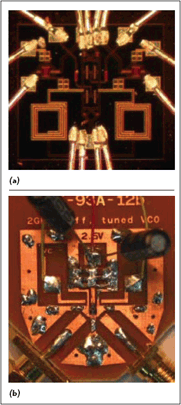
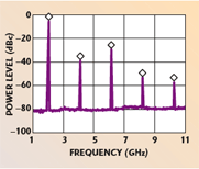
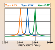
The VCO measurements were performed using an FR-4 PCB test fixture. Figure 4 shows the chip micrograph and a photograph of the FR-4 PCB test fixture. The VCO chip is connected to the test board with aluminum bond-wires. The effects of the bond-wires and the FR-4 test board were all taken into account in the simulation. The bond-wires and the FR-4 test board do not affect the oscillation frequency and phase noise performance; they only reduce the output signal amplitude. The VCO core and each buffer amplifier dissipate 8 and 16 mA, respectively, from a 2.5 V supply. The measured oscillation frequency of the VCO varies from 1827 to 2136 MHz when the differential control voltage varies from –1.25 to +1.25 V. The simulated and measured tuning ranges are shown in Figure 5. Figure 6 shows the simulated and measured VCO output power versus control voltage. The measured output power is approximately 8.2 dBm. Figure 7 shows a log plot of output phase noise measured with an Agilent E4440A spectrum analyzer with a phase noise utility program. The phase noise is approximately –100.2 dBc/Hz at 100 kHz offset from the carrier. The phase noise measurement was performed at the output frequency of 2050 MHz, where the VCO has the highest Kvco (~180 MHz/V) within the tuning range, which is for the worst case. Figure 8 shows the measured VCO output spectrum. The power level difference between the fundamental and second harmonic is approximately –36 dBc. Figure 9 shows the measured pushing figure, which is 9 MHz for a 0.2 V change in VDD. The figure of merit (FOM) of the VCO can be calculated from5


Conclusion
A 2 GHz CMOS complementary VCO, with differentially tuned MOS varactors fabricated with a TSMC 0.25 µm CMOS process, is presented. The VCO has demonstrated that differentially tuned varactors can provide a wide tuning range and reject the common-mode noise. The chip die size is 1.03 * 0.98 mm2, including the pads. The measurements were performed using an FR-4 PCB test fixture. The tuning range is 1827 to 2136 MHz, which is approximately 16 percent, with the control voltage varying from –1.25 to +1.25 V. The VCO output power is approximately 8.2 dBm while the second harmonic level is approximately –36 dBc below the fundamental. The phase noise is -100.2 dBc/Hz at a 100 kHz offset. The phase noise measurement was performed at 2050 MHz, where the VCO has the highest Kvco (~180 MHz/V) within the tuning range. Therefore, the phase noise is measured for the worst case. The pushing figure is 9 MHz per 0.2 V change in VDD. The power consumption is about 20 mW (without buffer) at VDD = 2.5 V.
Acknowledgment

The authors would like to thank the Chip Implementation Center of the National Science Council, Taiwan, ROC, for its support of the TSMC CMOS process.
References
1. J. Rogers, J. Macedo and C. Plett, “The Effect of Varactor Nonlinearity on Phase Noise of Completely Integrated VCOs,” IEEE Journal of Solid-State Circuits, Vol. 35, September 2001, pp. 1360–1367.
2. N. Fong, J.O. Plouchart, N. Zamdmer, D. Liu, L. Wagner, C. Plett and N.G. Tarr, “A Low Voltage Multi-GHz VCO with 58 Percent Tuning Range in SOI CMOS,” IEEE Custom Integrated Circuit Conference Digest, May 2002, pp. 423–426.
3. N.H.W. Fong, J.O. Plouchart, N. Zamdmer, D. Liu, L.F. Wagner, C. Plett and N.G. Tarr, “A 1 V 3.8 to 5.7 GHz Wideband VCO with Differentially Tuned Accumulation MOS Varactors for Common-mode Noise Rejection in CMOS SOI Technology,” IEEE Transactions on Microwave Theory and Techniques, Vol. 51, No. 8, August 2003, pp. 1952–1959.

4. A. Hajimiri and T.H. Lee, “Design Issues in CMOS Differential LC Oscillators,” IEEE Journal of Solid-State Circuits, Vol. 34, No. 5, May 1999, pp. 717–724.
5. T.J. Cho, S.Y. Oh, S.W Yoon, J. Laskar and R. Tummala, “Design of CMOS Voltage-controlled Oscillators using Package Inductor,” IEEE Electronic Components and Technology Conference Digest, Vol. 2, June 2004, pp. 1682–1686.
6. C.C. Ho, C.W. Kuo, C.C. Chih Hsia and Y.J. Chan, “A 2.4 GHz Low Phase Noise VCO Fabricated by 0.18µm PMOS Technologies,” IEEE International Symposium on VLSI Technology Digest, October 2003, pp. 144–146.
7. A.M. Thiebout, “Low Power Low Phase Noise Differentially Tuned Quadrature VCO Design in Standard CMOS,” IEEE Journal of Solid-State Circuits, Vol. 36, No. 7, July 2001, pp. 1018–1024.

Yuan-Kai Chu received his MSEE degree from National Cheng Kung University, Tainan, Taiwan, in 2002, where he worked on 5 GHz CMOS RFICs for his master studies. He is currently with the HiMAX Opto-electronics Corp. as an R&D engineer. His research interests include RFIC/MMIC design for wireless communication systems.
Huey-Ru Chuang received his BSEE and MSEE degrees from National Taiwan University, Taipei, Taiwan, in 1977 and 1980, respectively, and his PhD degree in electrical engineering from Michigan State University, East Lansing, MI, in 1987. From 1987 to 1988, he was a post-doctoral research associate at the Engineering Research Center, Michigan State University. From 1988 to 1990, he was with the Portable Communication Division of Motorola Inc., Ft. Lauderdale, FL. He joined the department of electrical engineering at National Cheng Kung University, Tainan, Taiwan, in 1991, where he is currently a professor. His research interests include antenna and RFIC/microwave circuit design for wireless communications, computational electromagnetics and applications, EMI/EMC, microwave communication and detection systems.


