GaN HEMTs have been considered to be the best option for realizing high performance in high power amplifiers (HPA), and now amplifiers based on GaN technology have started to become widely deployed in various applications. This article describes some development activities and performance results of GaN HPAs. The development of a high power added efficiency (PAE) process with a subsequent high output power amplifier for C-band space applications employing GaN HEMT technology is described. In this work, to boost the PAE, a newly introduced on-chip harmonic tuning for FETs is adopted. The 100 W HPA achieves a 67 percent PAE (72.4 percent drain efficiency) at 3.7 GHz, under CW operating conditions. To the best of the author's knowledge, this is the highest reported efficiency of C-band HPAs with over 100 W of output power. In other areas of development at other frequency bands, a 360 W L-band HPA having 65 percent PAE, and a 60 W X-band amplifier with 43 percent PAE are briefly described. The technologies, which have been developed for the 360 W L-band HPA, are particularly applicable for use in base station amplifiers suitable for the cellular phone network.
The GaN-based high electron mobility transistor (GaN HEMT) is generally considered to be the best choice in order to meet the requirements for many current HPA designs. HPAs have recently become desirable for high linearity and wider bandwidth operation at lower power consumption. While GaAs HEMT or LDMOS have traditionally been widely used as the HPA devices, GaN HEMT offers the following advantages:
- Higher PAE, which not only saves electrical power usage (OPEX), but also can reduce the size and cost of HPAs, due to the lower amount of heat dissipated (CAPEX).
- High operating voltage – GaN HEMT operates with a power supply voltage of up to 50 V, similar to the range of the power feeder voltage of 48 V, which is commonly used for communication equipment. Furthermore, for any given output power and supply voltage, the operating current can be reduced, when compared to other technologies.
In general, the amplifier design becomes more challenging as the transistor impedances become lower. GaN HEMT devices have a higher impedance than other technologies. Hence, the HPA design engineer can use the benefits of GaN to enhance HPA performance, such as wider frequency band coverage and higher PAE, depending on the required performance of the HPA.
In space applications, the vacuum tube based traveling wave tube amplifier (TWTA) is still used, because of a high PAE. However, because a TWTA needs an extremely high voltage, of the order of several thousands of volts, and reliability is considered not ideal due to the hot electrons in the vacuum tube, the solid-state power amplifier (SSPA) is often considered to be the favored solution. GaN based SSPAs are now in development, in order to replace TWTAs in many space applications and plans are in place to soon launch GaN SSPAs into space. In this article, a 67 percent PAE, 100 W GaN HEMT for C-band space use is described in detail.

Figure 1 GaN HEMT device structure cross-section.
GaN HEMT
Although the GaN HEMT was originally expected to be an ideal device for HPAs, early transistor designs raised the issue that the drain current measured under pulsed conditions was smaller than that observed under CW conditions. The phenomenon is called current collapse, and leads to a lower PAE and reduced output power. This was due to a less effective knee voltage, which reduced the maximum drain current. In order to suppress this current collapse, a SiN passivation film is deposited with a Cat-CVD process and NH3 treatments.1 In addition, Si ion implantation under the source and drain electrodes was employed to realize a low ohmic contact resistance.2 The GaN HEMT device structure employed in this work is shown in Figure 1. The gate-length is 0.6 μm and substrate via holes are used to produce higher power gain in the C-band.
Space Applications
In space applications, such as satellite communication systems, the RF power amplifier is one of the key components. In the amplifiers, a high PAE is important in order to reduce the launch cost of a satellite.3 C-band amplifiers, in the frequency range of 3.7 to 4.2 GHz, are often used for satellite downlinks.
In spite of the tremendous merits of SSPAs, GaAs based amplifiers cannot typically offer an acceptable PAE for many satellite applications and the GaN HEMT SSPA, with its higher PAE, is expected to be the best candidate for replacing TWTAs. Many organizations have recently developed GaN HPAs at C-band.4-8 However, there are very few reports for HPAs with more than 60 percent PAE.9

Figure 2 Second and third harmonic load/source pull measurements of a unit cell GaN HEMT.
HPA with high PAE
Figure 2 shows the second and third harmonic load/source pull measurements of a unit cell of a GaN HEMT (1.2 mm gate-width) with a PAE contour at an operating voltage of 40 V and a frequency of 3.7 GHz. Each measurement was performed while keeping the other fundamental and second and third harmonic impedances fixed for the maximum PAE. The figure shows that not only does the second harmonic output impedance have a substantial impact on PAE improvement, but so does the second harmonic input impedance. Moreover, the second harmonic input impedance region of the highest achieved PAE of more than 82 percent is near a short circuit and is a very small area when compared to the other impedance regions.
For the third harmonic, the contour of the high PAE is larger than that of the second harmonic. It is, therefore, important to precisely control the second harmonic input impedance to the short region. To achieve the high output power with higher PAE, many GaN-based amplifiers have adopted the harmonic impedance control technique, using resonance circuits such as open stubs formed on external matching circuits.4,9
However, this control is not easy to achieve, due to insufficient reflection of harmonic signals from the resonance circuit and the inductance of the bonding wire to the die. Moreover, the bonding wire brings an additional difficulty when trying to precisely control the reflected harmonic phase, because of the fluctuation in the bonding wire length at the second harmonic frequency.

Figure 3 Comparison of an adopted and conventional configuration.
Despite the higher impedance of a GaN HEMT compared to a LDMOS or GaAs HEMT, the above problem is more severe, particularly for a large gate-width FET amplifier, which consists of FETs connected in parallel. For this reason, it is not easy to realize a high PAE with the external harmonic matching circuits. In order to develop a 100 W GaN HPA for C-band space applications, an on-chip input second harmonic tuned FET technology for PAE improvement is introduced.

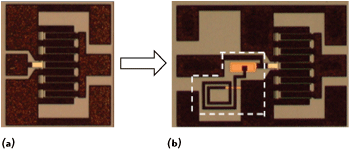
Figure 4 Comparison between a conventional FET (a) and an on-chip harmonic tuned FET (b).
Circuit Design
The simplified schematic of the adopted configuration, compared to a conventional configuration, is illustrated in Figure 3. In the case of the conventional amplifier, the second harmonic input impedance is controlled by the resonance circuit, such as open stubs, placed in the external matching circuit. As mentioned before, this configuration does not work well. In this study, the resonance circuit used for the second harmonic input impedance control is integrated in each unit cell placed on a GaN chip. The photographs in Figure 4 show the unit cell of a conventional FET and the on-chip harmonic tuned FET, respectively. In Figure 4b, the harmonic resonance circuit consists of a MIM capacitor and a spiral inductor, which are connected to the gate of the FET.

Figure 5 Comparison of PAE dependence with harmonic impedance.
In Figure 5, the PAE dependence on harmonic impedance is shown. The measurement conditions are the same as the conditions of Figure 2. When comparing performances of (a) the conventional FET and (b) the on-chip harmonic tuned FET, the on-chip harmonic tuned FET achieves the highest PAE of more than 82 percent at almost all second harmonic input impedances. Thus, this architecture is very effective for improving PAE, even in large gate-width FETs.

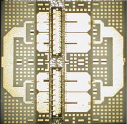
Figure 6 100 W GaN amplifier and FET chip.
Fabricated Amplifier Performance
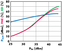
A 100 W amplifier was fabricated, using an on-chip harmonic tuned FET. The amplifier and FET chip are shown in Figure 6. The total gate-width of a single chip is 9.6 mm, and the chip size is 2.90 by 0.78 mm. The package size is 15.2 by 14.3 mm. The output characteristics versus input power are shown in Figure 7. For comparison, the performance of the highest PAE amplifier ever reported at C-band is also plotted. Both amplifiers were measured at 3.7 GHz under CW operation. The drain voltage and the quiescent drain current were 40 V and 2 A, respectively. As shown in the figure, a 67 percent PAE (72.4 percent drain efficiency) and a 107.6 W output power were obtained. The PAE is increased by more than five percent, when compared to the conventional amplifier,9 by using an on-chip harmonic tuned FET. Over the frequency range 3.65 to 4 GHz, this amplifier achieves a high PAE, greater than 60 percent, and a high output power greater than 100 W.

Figure 7 Output characteristics vs. input power (Vds = 40 V, 3.7 GHz, CW).
But because of the lower PAE of GaAs-based SSPAs, satellites continue to be launched into space using TWTAs. The new generation of GaN devices eliminates the issue of low PAE in SSPAs. GaN HEMT technology based SSPAs can now accelerate the replacement of the TWTA with the SSPA in these power ranges.
L-band GaN HEMT HPA
Considering other applications of GaN HEMTs, the HPA used in the base stations of the cellular phone network is well suited for the adoption of GaN. Currently, to improve the linearity of a HPA, Class AB operation is widely used, but Class AB results in less PAE and, therefore, consumes more power. Many studies using saturated amplifier designs have been carried out recently.10
The development results of a 65 percent PAE, 360 W, L-band saturation amplifier will now be covered. The technologies, which enable an increase in the output power and PAE, can be applied to enhance the performance of the main amplifier in a Doherty configuration for cellular phone base station amplifiers. A higher PAE is also important for the efficient performance of a remote radio head (RRH) scheme for base station architecture.

Among the high PAE HPA designs, Class E operation is the most popular approach for L- or S-band.10 In Class E amplifier design, the parasitic capacitance (Cp) of a transistor is used as the tank capacitance, which consists of an output matching network to achieve high efficiency. From theoretical analysis, the product of operation frequency and output power is inversely proportional to the Cp. In other words, the transistor technology with a smaller Cp can operate at a higher power or frequency.

As shown in Table 1, the Cp of a GaN HEMT is 23.6 times smaller than that of a LDMOS. Considering the current density and the capability of high voltage operation, the advantage of GaN HEMT over LDMOS is very attractive. Employing a modified Class E amplifier design, a 360 W L-band partially impedance matched GaN HEMT has been successfully developed. The load impedance for maximum PAE is shown in Table 2. A partially matched GaN HEMT and an external matching circuit for the 360 W L-band HPA were designed according to the best PAE points shown in the table. Figure 8 shows the GaN device and the external matching circuit. A packaged GaN HEMT with a partially matched circuit was attached to a heat sink by two screws. The GaN HEMT package can be seen between the external input and output matching circuits. The output characteristic of the L-band HPA is shown in Figure 9. The performance was evaluated with Vd = 56 V under pulse operation. The maximum output (Pout) was 360 W, with a PAE of 65 percent, or with a drain efficiency of 70 percent. Extending this developed technology, a 160 W partially matched GaN HEMT for CW operation has been developed, which is suitable for base station applications.

Figure 8 GaN device and external matching circuit.
This technology is applicable to modern linear amplifier design, which is needed in order to meet the high peak to average ratio (PAR) required by LTE. In satisfying the linearity requirement, GaN HEMT technology can offer a contribution toward increasing the PAE as well as reducing the amplifier size and cost. This is due to a lower heat dissipation, which is strongly required by the RRH configuration.

Figure 9 Output characteristics of the L-band HPA.

Figure 10 X-band HPA.
GaN HEMT HPA for X-band
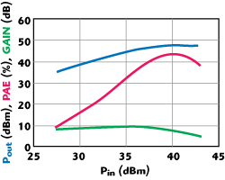
A high PAE HPA employing GaN HEMT is also desired for X-band. Therefore, an X-band amplifier has been designed and fabricated using a shorter gate length and narrow gate width in order to operate at a higher frequency. For X-band, the optimization of higher order harmonic frequencies is important, as it is for the lower bands. One advantage in designing for X-band is that harmonics are in the millimeter-wave region. Therefore, the harmonics have less influence on the PAE than for lower frequency bands, due to a relatively low emission output from GaN HEMT. However, due to the shorter wavelength, the difference in the path length between the matching circuit and the unit cells of the transistor does become a problem. This difference disturbs the equal distribution or combination of input/output power to/from each unit cell. The non-uniformity of power does not only result in a loss of power, but also necessitates an optimized unit cell impedance value. To overcome the problem, input/output matching circuits were designed in an asymmetrical manner in order to keep the uniformity of the power distribution/combination as shown in Figure 10. Figure 11 shows the output characteristics of the X-band HPA. The saturated output power reaches 60 W with a high PAE of 43.4 percent. These development results show that GaN HEMT is also well suited to operation at higher frequency bands.

Figure 11 Output characteristics of the X-band HPA.
Conclusion
GaN HEMT is the best transistor technology for producing high performance HPAs in many applications, so it can satisfy the market demands for high power, high PAE devices. For space applications, an HPA was developed, which offers 100 W output power, together with a very high efficiency of 67 percent. The performance improvements achieved in this development will help to accelerate the replacement of TWTA amplifiers with GaN based SSPAs in this power range.
At L-band, a 65 percent PAE, 360 W amplifier has been successfully developed. In this development, a modified Class E-amplifier technology has been applied for use in modern linear amplifier designs, such as in the main path of Doherty amplifiers. The use of GaN HEMT will encourage amplifier designers of RRH base stations, as used in the cellular phone network, to enhance amplifier performance in order to meet LTE requirements. The successful development of an X-band, 43 percent efficiency, 60 W HPA, shows the capability of GaN HEMT at high frequency bands.
References
- Y. Kamo et al., "A C-Band AlGaN/GaN HEMT with Cat-CVD SiN Passivation Developed for an Over 100 W Operation," 2005 IEEE MTT-S International Microwave Symposium Digest, WE1E-4.
- T. Nanjo et al., "Drivability Enhancement for AlGaN/GaN High-Electron Mobility Transistors with AlN Spacer Layer Using Si Ion Implantation Doping," Applied Physics Express, Vol. 2, No. 3, March 2009, pp. 031003-1-031003-3.
- R.K. Gupta, A. Vohra and V. Srivastava, "Efficiency Enhancement of C-band, 60 W Space Traveling Wave Tube (TWT)," Proceedings of the 2008 International Conference on Microwave, Recent Advances in Microwave Theory and Applications, pp. 288-290.
- H. Otsuka, K. Yamanaka, H. Noto, S. Chaki, A. Inoue and M. Miyazaki, "Over 57% Efficiency C-band GaN HEMT High Power Amplifier with Internal Harmonic Manipulation Circuits," 2008 IEEE MTT-S International Microwave Symposium Digest, WE1E-03.
- H. Shigematsu, Y. Inoue, A. Akasegawa, M. Yamada, S. Masuda, Y. Kamada, A. Yamada, M. Kanamura, T. Ohki, K. Makiyama, N. Okamoto, K. Imanishi, T. Kikkawa, K. Joshin and N. Hara, "C-band 340 W and X-band 100 W GaN Power Amplifiers with Over 50 Percent PAE," 2009 IEEE MTT-S International Microwave Symposium Digest, pp. 1265-1268.
- K. Krishnamurthy, J. Martin, B. Landberg, R. Vetury and M.J. Poulton, "Wideband 400 W Pulsed Power GaN HEMT Amplifiers," 2008 IEEE MTT-S International Microwave Symposium Digest, WE1E-01.
- K. Yamanaka, K. Mori, K. Iyomasa, H. Ohtsuka, H. Noto, M. Nakayama, Y. Kamo and Y. Isota, "C-band GaN HEMT Power Amplifier with 220 W Output Power," 2007 IEEE MTT-S International Microwave Symposium Digest, TH1A-2.
- Y. Takada, H. Sakurai, K. Matsushita, K. Masuda, S. Takatsuka, M. Kuraguchi, T. Suzuki, T. Suzuki, M. Hirose, H. Kawasaki, K. Takagi and K. Tsuda, "C-Band AlGaN/GaN HEMTs with 170 W Output Power," 2005 International Conference on Solid State Devices and Materials, Extended Abstracts, pp. 486-487.
- T. Yamasaki, Y. Kittaka, H. Minamide, K. Yamauchi, S. Miwa, S. Goto, M. Nakayama, M. Kohno and N. Yoshida, "A 68% Efficiency, C-Band 100 W GaN Power Amplifier for Space Applications," 2010 IEEE MTT-S International Microwave Symposium Digest, TH3D-1.
- N. Ui and S. Sano, "A 100 W Class E GaN HEMT with 75% Drain Efficiency at 2 GHz," 2006 European Microwave Integrated Circuits Conference Digest,pp. 72-74.
