Modern base station receivers for wireless communication infrastructures cope with extreme sensitivity and intermodulation characteristics, requiring sub 1 dB noise figures and high linearity for the low noise amplifier (LNA). Until recently, these specifications were only met using compound semiconductor technologies like GaAs PHEMT. However, NXP’s latest developments with their SiGe:C BiCMOS process, i.e. the QUBiC4X technology, speeds the migration from Gallium Arsenide (GaAs) to Silicon (Si) by offering comparable or better linearity, DC power consumption, immunity against out-of-band signals, spurious emission performance and increased output power.
To meet the demanding application requirements for wireless communication infrastructures, NXP has developed low noise, high linearity amplifiers (BGU705x series) in this SiGe:C BiCMOS technology with a high cut-off frequency (ft) of 130 GHz. A higher integration of circuitry is possible by this technology and covered in this product feature.

Figure 1 Maximum frequency up to which a certain NFmin is maintained for a given current (dotted lines: BNX device, solid lines: BNA device).
The first stage exists of a low-noise NPN BNX device with an emitter width of 0.4 µm and has an NFmin of 0.5 dB at 2 GHz for a current density of 0.25 mA/µm2 (see Figure 1). This current density will not deliver peak-ft, but the related ft is 30 GHz, still 10 times the operational frequency. Also, the available bandwidth for 10 times voltage gain is beyond 10 GHz for this current density. In other words, the device will certainly have more than 10 dB gain at 2 GHz. This low noise device can safely be operated at 3 V supply voltage. To achieve the high linearity performance requirements, a second stage is needed. Clearly, for sub 1 dB NF the noise contribution of the second stage remains important. If an overall NF of 0.6 dB is the target, the formula of Friis would require a NF of 0.7 dB for the second stage, assuming a realistic available gain of 15 dB in the first stage. The high voltage BNA device in this technology can still reach such a NF value, requiring a current density of 0.21 mA/µm2. The cut-off frequency for this device is then still 30 GHz.

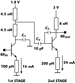
Figure 2 Schematic drawing of the LNA (biasing circuitry not shown).
The first stage uses inductive degeneration to get the input matched to 50 Ω. Inductive loading has been applied to realize 15 dB gain. Inter stage matching happens at a few ohms in order to improve linearity in the second stage. The second stage uses high voltage devices and measures an output third-order intercept point of +40 dBm, meanwhile having a noise figure of 0.7 dB. The output stage is directly matched to 50 Ω. A coarse overview of the design is shown in Figure 2 (biasing circuitry excluded).
Additional aspects such as ESD protection circuitry and I/O bond pads will influence the final design parameter choices. To minimize layout parasitic effects, routing has been performed in the thick top metal layer only. High quality MIM capacitors with 5 fF/µm2 density have been used. The implemented inductors have Q-factors above 15 at 2 GHz. The LNA is housed in a 10-terminal small, thin plastic outline package.

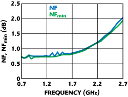
Figure 3 Measured NF and NFmin as a function of frequency at room temperature.
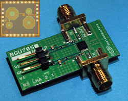
The resulting low noise, high linearity amplifiers meet the requirements of sub 1 dB noise figures (see Figure 3) and high linearity for wireless communication infrastructures. Additionally, compared to GaAs based discrete equivalents, these devices offer better DC power consumption, high immunity to high input level signals, spurious emission performance and increased output power. A demo board and die micro photo are shown in Figure 4.
The BGU7051 provides a typical low noise figure of 0.7 dB and high linearity output third-order intercept point of +32 dBm in the 750 to 900 MHz band. The associated gain is better than 20 dB typical and the 1 dB gain compression at the output is at 17 dBm. The input return loss is typically 25 dB.

Figure 4 Micro photograph of die (left) and demo board (right).
Similarly, the BGU7052 operates between the 1.5 and 2.5 GHz with a NF of 0.8 dB at 1900 MHz. Linearity performance is similar to the BGU7051. The BGU7053 offers comparable performance levels in the 2.3 to 2.8 GHz band. With the BGU705x series, the cellular frequency bands from 700 MHz up to 3.5 GHz can be covered. The BGU705x series is unconditionally stable and consumes less than 200 mW.
A new family of LNAs has been developed by NXP with low noise figures and high linearity using the SiGe:C BiCMOS technology. These devices compare well to compound semiconductor equivalents offering comparable or better linearity, DC power consumption, immunity against out-of-band signals, spurious emission performance and increased output power.
NXP Semiconductors
Eindhoven, The Netherlands
www.nxp.com
