Understanding device behavior under desired operating conditions is a critical step in the design of any high performance active RF device (e.g., an amplifier or converter). If the component operates in continuous-wave (CW) mode, that characterization can be as simple as measuring its S-parameters using a vector network analyzer (VNA). When it operates in pulsed mode, however, characterization is not so simple. In addition to S-parameters, many other active parameters must be measured in pulse mode. In the case of an amplifier, those parameters include the 1 dB compression (P1dB), intermodulation distortion (IMD) and third-order intercept point (IP3). The amplifier’s noise figure, higher-order distortion products and harmonics, among other things, may also be characterized depending on its intended application. Because these active parameters are power-dependent, additional considerations are needed to ensure precise characterization. Understanding the changes required to the VNA to support these measurements is also critical.
To better understand the challenge of accurately measuring pulsed active devices let us first look at the different pulsed operation modes: pulsed-RF and pulsed-bias. The pulsed-RF operation drives a device with a pulse-modulated RF signal and the DC bias is always on. Amplifiers used in receivers in pulse-modulated applications are typically tested under pulsed-RF operation, which requires RF pulse modulators for the stimulus and pulse generators to synchronize (or gate) the VNA receivers to capture the modulated RF signals.
With pulsed-bias operation, the DC bias is switched on and off to generate a pulse-modulated signal. The input is mostly a CW signal. Pulse generators may be needed to turn on and off the DC bias. The VNA receivers are synchronized to measure the output signal when the device is on.
For pulsed-RF network analysis, three types of measurements are performed—average pulse, point-in-pulse and pulse profile—using either wideband or narrowband detection techniques. Wideband detection is used when the pulse width is wide enough for VNA receivers to be able to measure the majority of the pulsed-RF spectrum. When the pulse width is too narrow, narrowband detection is used to measure only the center spectral response by removing all other pulsed-RF spectrum components.
VNA Considerations
When characterizing active devices in pulsed mode using either wideband or narrowband detection, there are a number of considerations that the engineer should keep in mind; namely, required changes to the VNA and techniques for enabling power-dependent active device characterization, including compression and distortion.

Active devices operating under pulsed conditions can be measured with a VNA, but some hardware modifications are required. For pulsed-RF operation, pulse modulators and generators must be added to the VNA. Pulsed-bias operation may require the addition of pulse generators. One example of an analyzer with integrated pulse generators and modulators is the Agilent Technologies’ PNA-X (see Figure 1). The internal pulse modulators and generators enable pulse measurements without external equipment, enabling precise pulse control, synchronization and fine timing resolution. Another required change to the VNA is the addition of a pulse input/output (I/O) port, which provides accessibility to internal pulse generators and modulators, and enables synchronous pulse measurements with external pulse generators or a device-under-test (DUT).

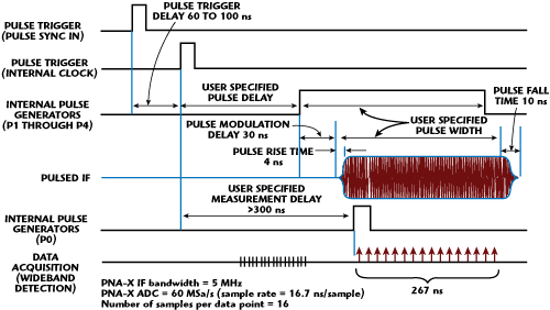
Figure 2 Timing diagram with 5 MHz BW from the external pulse trigger through the data.
An important consideration that must be taken into account when measuring active devices operating under pulse conditions is pulse system delays (e.g., delays in the pulse system from the pulse trigger to pulse generators, to pulse modulators, and to the ADC for data acquisition). Figure 2 shows a timing diagram with 5 MHz IF bandwidth, from the external pulse trigger through the data acquisition with wideband detection technique. Approximately 60 to 100 ns after the pulse trigger at the PULSE SYNC IN port, the internal pulse generators generate a pulse to drive the pulse modulator and the receiver data acquisition timing. The pulse modulator has about a 30 ns delay to modulate the RF signals. User-specified delays for pulse generators are used to adjust the modulation and measurement timings to account for pulse system delays. If any of the pulse system delays (e.g., pulse trigger and modulation delays), plus other system delays from the test port cables and DUT’s electrical length, are relatively long compared to the pulse width and the VNA’s receiver data acquisition time, then the timing of each must be carefully adjusted. Additionally, the data acquisition window should be placed at the middle of the pulses (approximately), and a wide enough IF bandwidth chosen to complete the data acquisition in approximately a half of the pulse width. By doing this, most timing errors can be avoided.
Power-Dependent Active Device Characterization
Devices that operate under pulsed condition are often discrete active devices or modules that consist of amplifiers and/or mixers. The performance of these devices is typically power-dependent. Therefore, they are characterized in linear and nonlinear operating conditions. Inaccurate stimulus power may introduce considerable measurement errors.
In some VNAs, the stimulus power is factory calibrated. This provides a reasonably accurate stimulus power level at the test ports, even without source power calibration. When accurate stimulus power is required at the device input (typically at the end of the test port cable), source power calibration is performed. The calibration compensates for the path loss and corrects errors, which in turn, enables the stimulus power accuracy to be set to a specified tolerance level from the power sensor accuracy. For pulsed-RF measurements, this simple calibration becomes problematic. Because most power sensors measure average RF power, the sensor readings are 10log(duty cycle) lower than the peak pulse power during source power calibration in pulse mode. Two approaches may be employed to overcome this source power calibration problem.
Source Power Calibration Using Power Sensor Loss
This technique is used to calibrate the stimulus with the pulse modulation on. To successfully perform a source power calibration, the power sensor loss feature must be used to ensure the VNA’s source does not go unleveled as it tries to bring the test port power to the desired calibrated power level. The pulse desensitization effect due to the pulse duty cycle appears as attenuation, thus the power offset is always negative. For example, the power offset value for a pulsed-RF stimulus with 5 percent duty cycle is 10log(0.05) = -13 dB.
Accurate Pulse Stimulus Using Receiver Leveling
The VNA receiver is used to monitor the pulsed-RF power and correct the source power level for every measurement sweep in receiver leveling mode. Once the receiver leveling is selected, the source level is adjusted with the receiver readings and the source power correction coefficients are ignored (source power calibration is not used even if it is turned on). Reference receivers are typically used for receiver leveling, although any receiver or even a power sensor (if added as a receiver to the VNA) can be used. The source level accuracy in receiver leveling mode depends on the receiver’s absolute power measurement accuracy, making receiver calibration essential.
Reference receivers can be calibrated by performing receiver calibration independently or as part of a source power calibration, although the latter is recommended. During calibration, the leveling mode must be open loop with the same source chain settings as the measurements, and the pulse modulation must be turned off. Also, the receiver setting must be the same between the receiver calibration and the pulsed measurements.
Once calibrated, the receiver can accurately measure the peak pulse power in wideband detection and adjust the source power until it is either in the specified tolerance or reaches the maximum number of iterations before the measurement sweep. In narrowband detection mode, the receiver measures the power lower than the peak pulse power by 20log(duty cycle). The power offset may be used with receiver leveling in narrowband pulse measurements.

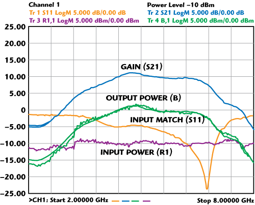
Figure 3 Calibrated wideband pulsed S-parameters and absolute power measurements with a companies between open loop and receiver leveling modes.
Note that for S-parameter measurements, where the DUT is in linear operation, power is not a concern and open loop leveling is suitable. When making absolute power and/or power-dependent performance measurements, the pulsed stimulus power matters greatly and must be accurately leveled. In this case (wideband detection), receiver leveling is recommended (see Figure 3). The difference in memory traces is very small in the input match and gain measurements, but is larger in the absolute power measurements. It can be used with both wideband and narrowband detection and applied to swept-power measurements, as well as compression and two-tone IMD measurements.
Accurately measuring pulsed active devices can be a difficult task, especially when those measurements are power dependent. Receiver leveling offers one means of addressing this issue. Another consideration the engineer must be aware of when characterizing active devices is selecting a VNA that supports pulse generators and modulators. Employing the right solution and appropriate techniques for accurately leveling the pulsed stimulus power are critical for enabling both S-parameter measurements and accurate power-dependent active device characterization, including compression and distortion.
