Bluetooth wireless technology is a short-range communications technology intended to replace the cables connecting portable and/or fixed devices while maintaining high levels of security. A Bluetooth device, as well as a cell phone, is often carried by people themselves, resulting in a very compact size requirement for the Bluetooth filter. However, continuing reductions in the size of discrete surface-mounted components have diminishing returns because of the incompatibility of the printed circuit board (PCB) technology.
Therefore, one of the important fabrication methods for compact size passive components, particularly for RF passive components, is the low temperature co-fired ceramic (LTCC) technique.1 Among the various LTCC passive components, people usually pay the most attention to filters.2-5 In microwave filters, the distributed element approach is often used to obtain lower insertion loss and better stopband performances. However, these designs exhibit comparatively large sizes, due to the fundamental disadvantage of using quarter-wave sections at relatively low frequencies. With the added new design dimension in the z-direction provided by LTCC, lumped-element RF filters have been implemented in stacked structures, which not only provide various coupling mechanisms to achieve better frequency selectivity, but also shrink the size.6-9
To obtain a sharper rate of cutoff and without using a higher order of filter, the method of zero transmission is adopted.7-8 Yeung and Wu7 have demonstrated that a filter with zero transmission not only has a better selectivity, but also has nearly the same pass band characteristics as those of traditional second-order coupled-resonator filters. However, good performance is achieved in the stop band; the overall size of the filter is 4.3 × 2.0 × 0.53 mm. Although Tang obtained better performance in the stop band and realized a more compact size8 (2.8 × 2.6 × 0.6 mm), the two transmission zeros appear on the same side of the pass band, so the characteristics of the other side of the stop band are poor. Recently, two new bandpass filters using third-order topology without transmission zeros have been reported.9 The new bandpass filters have desirable performance characteristics, but the overall sizes are 5 × 5.4 × 0.8 mm and 5 × 6 × 0.8 mm, respectively.
In this article, the inserted capacitance and inductance are modeled and the theory of transmission zeros is analyzed. A compact LTCC 2.45 GHz (the Bluetooth frequency) lumped-element bandpass filter with two transmission zeros is introduced. A prototype filter of size 3.0 × 1.5 × 0.5 mm (0.02λ × 0.01λ × 0.004λ) has been implemented in a multilayer LTCC substrate for experimental verification. It is believed that this is the minimum size for a bandpass filter operating at the center frequency of 2.45 GHz. The measured results show that the insertion loss is less than 4.8 dB and the return loss is better than 13 dB.

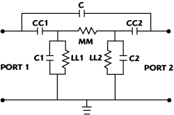
Figure 1 Schematic of a two-pole, second-order filter.

Figure 2 Alternative representation of the mutual inductor.
Model
The finite transmission zeros are mainly caused by blocking energy, so serial or parallel LC resonance circuits can be used in order to introduce a pair of finite transmission zeros. A well known two-pole filter schematic is shown in Figure 1.7 It consists of a second-order coupled resonator bandpass filter with a feedback capacitor. The purpose of the feedback capacitor C is to introduce a pair of finite transmission zeros to the transmission characteristics of the filter. The pass band characteristics will not be impacted by the feedback capacitor C. As shown, there is a mutual coupling M. To simplify the analysis, the circuit is transformed to the one shown in Figure 2, using the Y-to-Delta transformation. The values of the inductors in the representation configuration are given by7

where M is the mutual coupling, and L1 and L2 are the lumped inductors of the filter.
Simulation and Optimization
According to the above discussion, a bandpass filter with a 2.45 GHz center frequency and two transmission zeros has been designed. The substrate material is a ceramic, with a εr = 14 and a δ = 0.0015. Based on the synthesis method for a bandpass filter outlined by Sun, et al.,6 the normalized parameters of the second-order Chebyshev-type bandpass filter prototype circuit are g0 = 1, g1 = 1.0378, g2 = 0.6745 and g3 = 1.5386. After introducing the frequency, the component values are CC1 = CC2 = 0.85 pF, LL1 = LL2 = 1.64 nH, C1 = C2 = 2.25 pF and MM = 8.79 nH. The value of the feedback capacitor C can be selected depending on the desired locations of the transmission zeros.

Figure 3 3-D structure of the bandpass filter with two transmission zeros.
With the multilayer capability of the LTCC technology, the lumped-element model can be readily realized by using parallel plates for the capacitors and a metallic strip for the inductors. The structure of the lumped-element bandpass filter is shown in Figure 3. The up capacitor and down capacitor are a parallel connection, and the inductor is implemented by a single layer spiral inductor. The size of the inductor and the capacitor can be initially obtained from Equations 2 and 3

where Ceff is the capacitance of the capacitor, n is the number of layer of the capacitor, εr is the relative permittivity of the medium, S is the area of the plate and d is the distance between two adjacent plates.

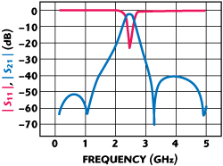
Figure 4 Simulated results for the bandpass filter with two transmission zeros.
As shown in the figure, there are seven layers in the LTCC structure; the height of every layer is 0.006 mm. The top and the bottom layers are the grounded plates. The second and sixth layers are the parallel capacitors C1 and C2, respectively. The third layer is the feedback capacitor C, using a dumbbell shape. The fourth layer is composed of inductors LL1 and LL2, which are coupled to each other to fulfill the coupling inductor MM. One port is grounded and the other port is connected to C1 and C2 by the through hole. The fifth layer is composed of the input capacitor CC1 and output capacitor CC2.
The final structure was simulated and optimized using the 3-D full-wave electromagnetic (EM) simulation tool Ansoft HFSS. The simulation results are shown in Figure 4. It can be seen that the center frequency is 2.45 GHz, the insertion loss in the pass band is less than 2 dB and the return loss is better than 20 dB. Additionally, there are two transmission zeros at 1.1 and 3.2 GHz, respectively.

Figure 5 Photograph of the fabricated filters.
Fabrication and Measurements
The final filter has been designed and built in an LTCC format using Ferro ULF140 with a εr = 14 and aδ = 0.0015. Before designing the silk screen, attention should be paid to the shrinkage rate of the ceramic ULF140. The filter has employed a lumped-element envelop 1206 (3.0 × 1.5 × 0.5 mm) and has been fabricated at the LTCC Engineering Center, University of Electronics Science and Technology of China (UESTC). A photograph of the filter is shown in Figure 5.
The measurements were performed by connecting a test fixture provided by the LTCC Engineering Center of UESTC to the two external ports of the filter. The frequency response of the filter was measured using a network analyzer Agilent 8722ES; the measured curves are drawn in Figure 6. As can be seen, the measured insertion loss of the filter is less than 4.8 dB and the return loss is better than 13 dB within the passband. The stopband (lower than 1.8 GHz and higher than 3.6 GHz) rejection is greater than 30 dB. However, the measured center frequency shifted from the simulated 2.45 to 2.69 GHz. It may be due to the ceramic sintering process failing to reach the appropriate temperature, resulting in an undesired dielectric constant. On the other hand, the transmission zeros shown in the simulation do not show up in the measured data. The reason may be that the screen design is based on the average rate of contraction, but the experimental sintering shrinkage rate did not achieve the desired result, so that the capacitance of the feedback capacitor is reduced.

Figure 6 Measured results for the bandpass filter.
Conclusion
By introducing a feedback capacitor, a lumped-element bandpass filter with dual transmission zeros and using LTCC technology is presented. The filter is simulated and optimized with the 3-D electromagnetic code Ansoft HFSS for a center frequency of 2.45 GHz. In order to verify the design, the filter was fabricated using LTCC technology. The test results show that the filter has good transmission characteristics, with a pass band insertion loss less than 4.8 dB and a return loss better than 13 dB. The device has a compact size of 3.0 × 1.5 × 0.5 mm (0.02l × 0.01l × 0.004l). The filter has promising potential to be applied to the increasingly widespread use of Bluetooth devices and other mobile communications equipment.
References
- B. Vorotnikov, A. Chernyakov, S. Sakhnenko, A. Yatsenko, G. Sevskiy and P. Heide, "High Performance 2.4 GHz Combined LTCC/SAW Filter for WLAN Applications in Mobile Phones," 2007 European Microwave Conference Proceedings, pp. 438-441.
- Z. Wang, X. Zeng, B. Yan, R. Xu and W. Lin, "A Millimeter-wave E-plane Bandpass Filter Using Multilayer Low Temperature Co-fired Ceramic (LTCC) Technology," Journal of Electromagnetic Waves and Applications, Vol. 24, No. 1, 2010, pp. 71-79.
- J. Gu, Y. Fan and Y. Zhang, "An X-band 3-D SICC Filter with Low Loss and Narrow Band Using LTCC Technology," Journal of Electromagnetic Waves and Applications, Vol. 23, No. 8-9, 2009, pp. 1093-1100.
- Y.C. Zhang, K.A. Zaki, A.J. Piloto and J. Tallo, "Miniature Broadband Bandpass Filters Using Double-layer Coupled Stripline Resonators," IEEE Transactions on Microwave Theory and Techniques, Vol. 54, No. 8, August 2006, pp. 3370-3377.
- Q.F. Wei, Z.F. Liand L. Li, "Three-pole Cross-coupled Substrate-integrated Waveguide Bandpass Filters Based on PCB Process and Multilayer LTCC Technology," Microwave and Optical Technology Letters, Vol. 51, No. 1, January 2009, pp. 71-73.
- X.L. Sun, H. Huang, M. Zhu, H.Y. Zhuang and H.D. Liu, "Design and Realization of an LTCC Bandpass Filter," Chinese Journal of Electron Devices, Vol. 31, No. 6, 2008, pp. 1864-1866.
- L.K. Yeung and K.L. Wu, "A Compact Second-order LTCC Bandpass Filter with Two Finite Transmission Zeros," IEEE Transactions on Microwave Theory and Techniques, Vol. 51, No. 2, February 2003, pp. 337-341.
- C.W. Tang, "Development of LTCC Bandpass Filters with Transmission Zeros," Electronics Letters, Vol. 43, No. 21, October 11, 2007, pp. 1149-1150.
- G. Brzezina, L. Roy and L. MacEachern, "Design Enhancement of Miniature Lumped-element LTCC Bandpass Filters," IEEE Transactions on Microwave Theory and Techniques, Vol. 57, No. 4, Part 1, April 2009, pp. 815-823.
