To meet the ever-increasing demands of next generation wireless infrastructure, fiber optics and advanced military systems markets, WIN Semiconductors Corp. has developed an ultra-high performance 0.1 µm GaAs PHEMT technology. This device platform, named PP10, is produced on 150 mm GaAs wafers in WIN Semiconductor’s state-of-the-art wafer foundry located in Taiwan and is available with an option of 50 or 100 µm substrate thickness. With Ft greater than 135 GHz and Fmax over 185 GHz, PP10 is targeted towards millimeter-wave power products at E- and V-band, and will enable the realization of high data rate 70 to 90 GHz point-to-point radios used in the backhaul of 3G/4G mobile base stations. Additionally, the superior performance of PP10, as well as the volume availability of products built on this technology will make possible a wide range of high frequency products in entirely new applications.
PROCESS DESCRIPTION
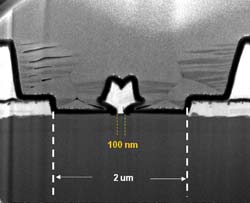
The PP10 process leverages an advanced materials design with electron-beam defined 0.1 µm gates and a qualified 150 mm manufacturing infrastructure to obtain a high volume, ultra-high performance technology platform. The critical 0.1 µm T-shaped gate is defined in a Leica direct-write E-beam lithography system. The e-beam lithographic process has been optimized to enable a wafer to be patterned in less than 30 minutes and provides more than adequate throughput to support volume production of 0.1 µm gate products. The electron beam lithography process forms the 0.1 µm T-Gate profile, which simultaneously provides the short gate length necessary for high frequency operation and a low gate resistance. The high pattern accuracy and resolution capabilities of E-beam patterning is illustrated in the cross-section shown above, which shows a typical PP10 gate with a 0.1 µm foot and 0.5 µm top dimension positioned within the 2 µm drain-to-source spacing. PP10 has been designed with a 2 µm source to drain spacing and uses a single recess channel geometry to achieve optimum current/transconductance characteristics while maintaining an adequate breakdown voltage for reliable 4 V operation.
As with all high performance technology platforms built by WIN Semiconductors, the transistor cells employ through the substrate source vias and airbridge connections to reduce parasitic capacitances. Additionally, the MMICs are fully passivated using silicon nitride deposited via PECVD and is used as the dielectric for standard 400 pF/mm2 Metal-Insulator-Metal (MIM) capacitors.
To provide the product designer additional flexibility, PP10 is available with a 100 µm wafer thickness as well as the production proven 50 µm substrate option. WIN Semiconductors has been producing high yield 50 µm thickness 150 mm diameter GaAs wafers for more than 10 years, providing customers with volume availability of this advantageous design option. The 50 µm substrate thickness provides better thermal management in the package and better confinement of electric fields on microstrip line designs and is especially important for the 60 to 90 GHz frequency range. At the same time, the smaller size of backside via available at the 50 µm wafer thickness provides a reduction in the gate-to-gate pitch for better signal coherence between each single transistor cell.
DC AND RF PERFORMANCE

Figure 1 The 7 V I-V curve (a) and MSG (b) of the PP10 process.
DC I-V curves of a typical 2 x 50 µm PP10 device is shown in Figure 1. The IV characteristics are well behaved and exhibit a nominal pinch off voltage of -0.9 V, peak transconductance of 750 mS/mm and a maximum current density of 720 mA/mm (measured at Vgs=0.5 V). The material and device design produces a knee voltage of less than 1 V and a typical gate-to-drain breakdown voltage greater than |9 V| providing large available current and voltage swing for the RF signal, and very high power density under 4 V operation.

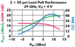
Figure 2 29 GHz power performance of PP10.
S-parameter measurements taken at Vds= 2 V and extraction of Maximum Stable Gain (MSG) to 110 GHz is shown in Figure 2 for both 2 x 25 µm and 2 x 50 µm transistors. These data show the PP10 devices provide 9 to 10 dB gain from 70 to 90 GHz; the 2 x 25 µm transistor provides approximately 8 dB gain at 110 GHz. Load pull measurements for a 2 x 50 µm transistor taken at 29 GHz are shown in Figure 2 and illustrate the power capability of PP10. These measurements are taken at Vds=4 V and show excellent RF performance with a saturated power density of 850 mW/mm with a gain of 12 dB and peak power added efficiency (PAE) of 50 percent.

Figure 3 26 to 40 GHz noise performance of PP10.
The physical tradeoffs that accompany a power device designed for E-band (high gain, high available current) also provide for excellent noise performance. Shown in Figure 3 are measured Fmin and associated gain from an 8 x 25 µm PP10 transistor taken at a bias Vds=2 V and 50 mA/mm. From the data of Figure 3, one observes that PP10 also demonstrates excellent noise performance with a minimum noise figure of 0.8 dB and associated gain over 9 dB at 40 GHz. The confluence of high power density, superior gain and excellent noise performance of the PP10 technology allows the product designer to realize a highly integrated multifunctional device with high power amplifier, medium power amplifier and low noise amplifier on one chip for the E-band to V-band Tx/Rx core circuit, and is simply not possible in a technology of lesser performance.
WIN Semiconductors has developed and released an ultra-high performance 0.1 µm PHEMT technology for E-band power products. This technology platform is produced exclusively on 150 mm diameter GaAs wafers and is available in 100 and 50 µm wafer thickness for added product flexibility. The PP10 process offers WIN’s customers an optimum combination of excellent power and gain performance through 110 GHz as well as very low noise figure enabling highly integrated multifunctional products. By taking advantage of WIN Semiconductor’s high volume manufacturing infrastructure and short cycle times, the company’s customers can leverage PP10 to produce highly differentiated products for new high frequency applications and markets.
Acknowledgment
WIN would like to thank Robin Sloan of Manchester University UK for the support on the 110 GHz S-parameter measurements.
WIN Semiconductors Corp.,
Tao Yuan Shien, Taiwan
886-3-397-5999
info@winfoundry.com
www.winfoundry.com
RS No. 305
