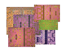
United Monolithic Semiconductors (UMS) has a considerable heritage in the design and production of MMIC solutions for space and defense programs. This extensive experience has been used to design state-of-the-art chipset for phased-array radar for defense, space and communication applications. The basic building block for such systems is a T/R module (see Figure 1) containing MMICs for control and amplification for both transmit and receive paths.
The company's X-band T/R module solutions, composed of a low noise amplifier (LNA), a core chip and a set of high efficiency high power amplifiers (HPA) from 8 to 10 W are based on in-house fully qualified and space evaluated processes. A high volume, single recess 0.25 μm gate length PHEMT process is used for the LNA and core chips. Two processes are used for the power amplifiers: a double recess 0.25 μm gate length power PHEMT process offering high power density (850 mW/mm) and high efficiency, and a GaInP/GaAs HBT process with high power density (3.5 W/mm) and high efficiency. This technology has been optimized for high reliability and includes specific features to reduce the junction temperature and increase the thermal stability of the device.

Figure 1 T/R module block diagram.
LNA and Core Chips
The CHA1014 is a 7 to 14 GHz, 50 Ω matched LNA designed to be used with the CHC3014 multifunction chip or in more general-purpose applications. It includes two amplification stages and a biasing circuit that compensates the spread in the technology. The LNA presents a very flat linear gain of 17 dB, a 1.5 dB noise figure, very good matching, better than 14 dB, and a +10 dBm output power at 1 dB gain compression.

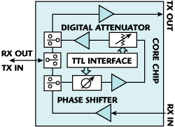
Figure 2 Core chip block diagram.
The CHC3014, whose schematic is presented in Figure 2, is a 22.7 mm2 transmit receive core chip including a 6-bit phase shifter, a 6-bit attenuator and two tuning bits chain gain tuning. The phase shifter and attenuator can be used in both Tx and Rx modes. A three-port switch with a Rx input, a Tx output and a common Rx output and Tx input port enables the commutation between three modes: Rx, Tx and neutral. The switch is matched to 50 Ω for all modes. The CHC3014 integrates parallel interfaces for the control functions, enabling easy implementation.

Figure 3 Phase shifter RMS phase error and attenuator RMS attenuation error.
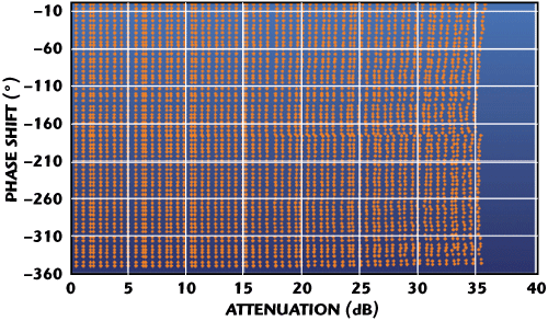
The device also includes buffer stages to provide 12 dB gain in Rx mode and a high Tx mode gain of 25 dB with very good matching. The return losses in all states are better than 14 dB in Rx mode and 12 dB in Tx mode. The phase shifting is 0° to 360° with a phase step of 5.625°. The peak phase error is typically better than ±6°, with a RMS error of 2°, associated with a low amplitude variation of ±1 dB.
The 6-bit attenuator provides a high attenuation range of 34.5 dB and a very good accuracy with an attenuation error of typically -1.5 to +1 dB (0.3 dB RMS). It also presents a very low phase variation versus attenuation setting; lower than 10° in any attenuation state. The 2-bit tuning attenuator with 2 dB step offers ±0.3 dB attenuation error and ±2° of phase variation. The core chip performances are presented in Figures 3 and 4.

Figure 4 Phase shift vs. attenuation diagram.
The output power is 19 dBm in Tx mode and 16.5 dBm in Rx mode. The Tx path has been designed for a very high robustness against overdrive. A very wide input power range, from 0 to 16 dBm, can be used as a standard saturated operating mode.
High Power Amplifiers
The X-band chipset includes a family of robust and efficient HPAs that are designed to deliver an output power from 8 to 10 W at 3 dB gain compression with a very high power added efficiency and a high robustness against power overdrive or mismatch.

Figure 5 CHA7115 linear gain, ouput power and PAE @ 3 dBc.
The CHA7115 and CHA7215 three-stage amplifiers are 30 percent frequency band amplifiers that are compatible with the CHC3014. They present a high linear gain of 28 dB. The output power delivered is 8 W for the CHA7115 and 9 W for the CHA7215 with a high power added efficiency of 40 and 35 percent, respectively. The performance of the CHA7115 is shown in Figure 5. The chip sizes are 15.2 and 16.55 mm2.
A 10 W power chain is also available with the 1 W driver CHA5014 and the 10 W HPA CHA8100, used together with the CHC3014. These two amplifiers integrate on-chip high impedance biasing control circuits and digital interfaces. The use of the biasing control circuit results in significant advantages; for example, efficient limitation of current variation due to temperature or technological spread and very good linearization of the collector current control.
Due to its high impedance, the decoupling in the circuit environment is straightforward. An integrated TTL interface connected to the control circuit using external bonding wires enables the switching of the HPA with a current consumption lower than 1 mA.

Figure 6 CHA8100 linear gain, output power and PAE @ dBc.
The CHA5014 and CHA8100 are 25 and 15 percent frequency band two-stage amplifiers, respectively, presenting 20 and 18 dB linear gain. The CHA5014 output power at 1 dB gain compression is 29 dBm with an associated power added efficiency of 35 percent. It also offers high power and efficiency compensation versus temperature, lower than 0.2 dB for power and lower than three points for PAE, in a 120°C temperature range. The CHA8100 provides 10 W at 3 dB gain compression and up to 11 W in saturation with a power added efficiency above 40 percent, as shown in Figure 6.
The robustness constraints versus overdrive or mismatch were parts of the targeted performances, as was the power and efficiency, and were an integral part of the design approach from the beginning. This results in a family of very high performance HPAs in terms of power, efficiency and robustness. All these HPAs can support up to 6 dB gain compression at -40°C on a load mismatch of 2:1.
Conclusion
UMS has developed a complete solution for high performance T/R modules based on internal fully qualified and space evaluated processes. This highly integrated solution (maximum system integration, reduced size) has been fully evaluated in production, is cost effective, easy to implement and suited for phased-array radar applications with high robustness and integrated TTL interface on chip.
United Monolithic
Semiconductors SAS,
France,
Tel: +33 (0)1 69 33 04 72;
E-mail: mktsales@ums-gaas.com;
UMS GmbH,
Germany,
Tel: +49 731 505 3002;
E-mail: mktsales@ums-gaas.com;
UMS USA Inc.,
USA,
Tel: (978) 905-3165;
E-mail: sales@us.ums-gaas.com;
UMS, PR
China,
Tel: +86 21 6103 1703;
E-mail: mktsales@ums-gaas.com.
RS No. 301
