Ultra-wideband (UWB) technology has been a key issue in the development of new high speed indoor and hand-held wireless communication systems since the unlicensed use of UWB was approved worldwide. As one of the essential components in UWB communication systems, the UWB bandpass filter (BPF), with such characteristics as compact size, good selectivity and stop-band rejection, low insertion loss and low cost, has been required. In order to meet UWB radiation limits, steep selectivity at lower and upper ends of the passband is a characteristic of UWB systems that must be obtained.1
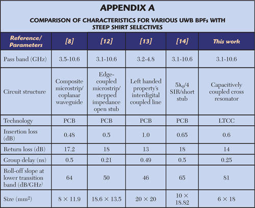
After Saito first introduced a UWB BPF, a number of reports on UWB BPF research and development have been published.2-14 In these reports, filters show steep skirt selectivity and compact size.8,12-14 The filter characteristics, in terms of passband, circuit structure, fabrication technology, insertion loss, return loss, group delay, roll-off slope at lower transition band and size, are compared in Appendix A, which also includes results of this work, using a capacitively coupled cross resonator.
A new UWB BPF with steep slopes, such as 81 dB/GHz in the lower transition band and 86 dB/GHz in the upper band, is proposed in this article. The design theory for the cross resonator-based UWB BPF is introduced. It explains how to obtain two attenuation poles based on a capacitively coupled cross resonator, how to add input and output lines, and how to obtain the UWB BPF for the frequency range from 3.1 to 10.6 GHz using an ABCD matrix method and ADS simulation. The HFSS simulation and measurement results for the BPF are given and compared.

Figure 1 Schematic of the proposed filter.
Design Theory
The configuration of the filter developed in this study is shown in Figure 1. The filter consists of a λ/2 long resonator, capacitively cross coupled with a λ/8 open-circuited stub on one side and a λ/8 short-circuited stub on the other side. The two stubs are located at the center of the resonator. Two identical λ/4 capacitively coupled lines are used at the input and output ports. The filter has been designed for the US UWB band, with a 6.85 GHz center frequency. The filter circuit is designed in a two-layer structure to obtain the capacitive coupling.

Figure 2 Capacitive coupling between the mainline and the cross resonator structure.
The filter design starts with the analysis of the even- and odd-modes for the coupling structure between the main line (empty section) and the cross resonator (shaded section), as shown in Figure 2. It also shows the one-port circuit model for the circuit structure under even-mode excitation. In this case, the symmetrical plane becomes a perfect magnetic wall. The characteristic impedances for the short-circuited stub and open-circuited stub are doubled (2Z1, 2Z2) and the main line on the upper layer becomes open-circuited. Therefore, the input impedance (Zine) can be derived, as shown in Equation 1

Zce and Zco are the even- and odd-mode impedances of the coupled line, Z1 and Z2 are the characteristic impedances, and θ1 and θ2 the electrical lengths of the short-circuited and open-circuited stubs, respectively.
Under the odd-mode excitation, the coupling structure is also expressed as a one-port network. In this case, the circuit at the symmetrical plane can be simply considered as short-circuited, since the strip conductors at the center are grounded via virtual electric wall. Therefore, the input impedance (Zino) can be obtained from Equation 2
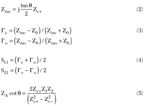

Figure 3 Locations of lower and upper transmission zeros depending on the electrical lengths of the stubs: (a) short-circuited stub and (b) open-circuited stub.
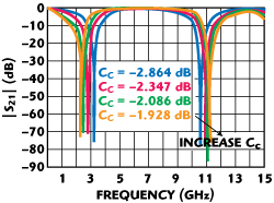
Figure 4 Location of the lower and upper transmission zeros depending on the coupling coefficient Cc.
Next, the reflection coefficients for the even-mode (Γe) and the odd-mode (Γo) can be determined from Equation 3. S11 and S21 of the capacitive coupled cross resonator structure can then be extracted from Equation 4. At the transmission zeros frequencies, S21 is equal to one. Therefore, the locations of the transmission zeros of the proposed filter are obtained from Equation 5. These transmission zeros depend on the coupling coefficient between the main line and the cross resonator and the impedances and lengths of the stubs. As shown in Figure 3, the location of the lower transmission zero can be controlled by the electrical length θ1 of the short-circuited stub and the upper transmission zero by the electrical length θ2 of the open-circuited stub, where θ0 = π/2 at the center frequency. The smaller the value of θ1, the higher the frequency of the lower transmission zero. In contrast with θ1, the smaller the value of θ2, the lower the frequency of the upper transmission zero. The other circuit parameters are: Wc1 = Wc2 = 0.35 mm, offc = 0 mm, W1 = W2 = 0.5 mm and θ0 = π/2. Figure 4 shows the location of the lower and upper transmission zeros depending on the coupling coefficient Cc between the main line and the cross resonator when the other parameters are Wc1 = Wc2 = 0.15 to 0.45 mm, offc = 0 mm, W1 = W2 = 0.5 mm, θ0 = π/2 and θ1 = θ2 = π/4.
Finally, the input and output lines coupled with the main line of the coupling structure have been adopted to suppress the unwanted signals in the lower and upper stop-bands. To obtain rejection bands better than 25 dB, the impedances of the even- and odd-modes of the input/output coupled lines are set at 90.3 and 22.96 Ω, respectively. Then, the 50 Ω input and output transmission lines are connected to the coupled lines. In this study, the stripline structure with a substrate thickness of 0.6 mm, a dielectric constant of 7.8, a conductor thickness of 10 μm and a capacitive coupling gap of 43 μm were used. By choosing Zce = 55.87 Ω and Zco = 5.95 Ω, Z1 = Z2 = 25.51 Ω, θ1 = θ2 = π/4, the two transmission zeros have been placed at 2.5 and 11.1 GHz.
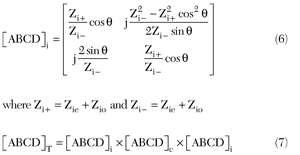

Figure 5 ADS simulation results for the proposed filter.
The [ABCD]c matrix of the capacitively coupled cross resonator structure can be calculated from its S-parameter in Equation 4.15 The [ABCD]i matrix of the coupled lines at the input or output can be written as Equation 6, where Zie and Zio are the even- and odd-characteristic impedances of the coupled lines. Correspondingly, the [ABCD]T matrix of the whole filter can be obtained by Equation 7, which is the multiplication of the transmission matrix of the cross resonator structure [ABCD]c and those of the input/output coupled lines with Equation 6 in sequence. Finally, the scattering matrix for the whole filter structure can be obtained.15 Figure 5 shows the ADS simulation results for the proposed bandpass filter. The filter shows a bandwidth from 3.1 to 10.6 GHz with the two transmission zeros at 2.5 and 11.1 GHz.
The ADS (Agilent, 2008) simulation results of the filter show a flat and wide passband characteristic for US UWB applications and effectively suppressed unwanted passbands in the lower and upper stop-bands.
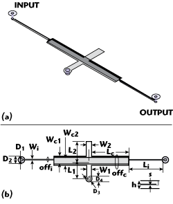
Figure 6 The structure of the cross resonator filter: (a) 3-D view and (b) top view.
Field Simulation and Measurement Results
The filter structure with the cross resonator, shown in Figure 6, was simulated and tuned with the HFSS program (Ansoft, v.11). Its dimensions are: Wi = 70 μm, offi = 0 mm, Li = 3.9 mm, Wc1 = Wc2 = 0.5 mm, offc = 60 μm, Lc = 3.8 mm, W1 = 0.5 mm, L1 = 1.7 mm, W2 = 0.55 mm, L2 = 2 mm, D1 = 0.2 mm, D2 = 0.75 mm, D3 = 0.4 mm, D4 = 0.55 mm, h = 0.6 mm and s = 43 μm.
The structure consisted of 14 layers; each layer had a thickness of 43 μm and a dielectric constant of 7.8. The filter patterns were located on the sixth and seventh layers. Via holes were added to the structure instead of solid walls in order to reduce the effects of interference. Due to the limitations of the LTCC manufacturing process used, the distance between two adjacent vias needed to be larger than 0.35 mm. This led to a slight deterioration of the performance of the filter such as the disappearance of the fourth transmission poles in the passband.

Figure 7 Comparison between measured and simulated results for the proposed filter.
The filter characteristics were measured with the Anritsu ME7808A network analyzer and the Cascade Microtech Summit 12971B probe station. The measurement results were compared with the simulation results. The input/output striplines were connected to input/output circular ports, which have inner and outer diameters of 200 and 750 mm, respectively, by solid vias (via diameter of 120 μm). The measurement probes with a 400 μm pitch size were used to measure the filter. Figure 7 shows the comparisons between the simulation and measurement results in terms of S-parameters and group delay for the filter. The dotted line indicates the simulation results. The simulation results show a bandwidth of 7.5 GHz (3.1 to 10.6 GHz). The return loss is better than 15 dB, and insertion loss is less than 0.3 dB in the passband. The group delay of the filter is approximately 0.26 ns at 6.85 GHz and has a variation within 0.25 ns from 3.5 to 10.2 GHz. The attenuation slopes in the lower and upper transition bands are 94 and 95 dB/GHz, respectively. The filter has two transmission zeros at 2.45 and 11.05 GHz, respectively.

Figure 8 Top view of the fabricated bandpass filter.
The solid line shows the measurement results. Due to the limitation of the LTCC fabrication process mentioned before, the second and third poles were smeared, so only four poles instead of five poles can be observed within the passband in the measurement result. A return loss better than 14 dB and an insertion loss less than 0.6 dB were measured. The group delay is 0.26 ns at the center frequency and the group delay variation from 3.5 to 10.2 GHz is less than 0.25 ns. The attenuation slope in the lower transition band is 80 dB/GHz and that in the upper transition band 86 dB/GHz. The proposed filter has a size of 6 × 18 × 0.6 mm3 and shows very sharp skirt characteristics with transmission zeros at the lower and upper stop-bands. Figure 8 shows the top views of the fabricated bandpass filter.
Conclusion
In this article, a UWB bandpass filter with sharp frequency characteristics for the US band was introduced in LTCC technology. It is shown that the capacitive coupling of the cross resonator provides ultra-wideband characteristics. Locations of two transmission zeros in the lower and upper transmission bands of the filter can be controlled by the capacitive coupling coefficient between the main line and the cross resonator, and the lengths of the short-/open-circuited stubs. The HFSS simulation results agree well with the measurement results. It is expected that the sharp roll-off characteristics and simple structure of the filter make it very suitable for UWB systems, particularly in mobile home network applications.
Acknowledgments
The authors wish to acknowledge the financial support of LG Innotek and the measurement assistance of the Korea Electronics Technology Institute (KETI).
References
- "Revision of Part 15 of the Commissionís Rules Regarding Ultra-wideband Transmission System," Federal Communications Commission, 2006 [Online], available: http://ftp.fcc.gov/oet/info/rules/part15.
- A. Saito, H. Harada and A. Nishikata, "Development of Bandpass Filter for Ultra-wideband (UWB) Communication Systems," Proceedings of the 2003 IEEE Conference on Ultra-Wideband System Technology, pp. 76-80.
- H. Ishida and K. Araki, "Design and Analysis of UWB Bandpass Filter with Ring Filter," 2004 IEEE MTT-S International Microwave Symposium Digest, pp. 1307-1310.
- C.L. Hsu, F.C. Hsu and J.T. Kuo, "Microstrip Bandpass Filter for Ultra-wideband (UWB) Wireless Communications," 2005 IEEE MTT-S International Microwave Symposium Digest, pp. 679-682.
- L. Zhu, S. Sun and W. Menzel, "Ultra-wideband (UWB) Bandpass Filters Using Multiple Mode Resonator," IEEE Microwave and Wireless Components Letters, Vol. 15, No. 11, November 2005, pp. 796-798.
- H. Wang, L. Zhu and W. Menzel, "Ultra-wideband Bandpass Filter with Hybrid Microstrip/CPW Structure," IEEE Microwave and Wireless Components Letters, Vol. 15, No. 12, December 2005, pp. 844-846.
- J. Gao, L. Zhu, W. Menzel and F. Bogelsack, "Short-circuited CPW Multiple-mode Resonator for Ultra-wideband (UWB) Bandpass Filter," IEEE Microwave and Wireless Components Letters, Vol. 16, No. 3, March 2006, pp. 104-106.
- T. Kuo, S. Lin and C.H. Chen, "Compact Ultra-wideband Bandpass Filters Using Composite Microstrip-coplanar-Waveguide Structure," IEEE Transactions on Microwave Theory and Techniques, Vol. 54, No. 10, October 2006, pp. 3772-3778.
- R. Li and L. Zhu, "Compact UWB Bandpass Filter Using Stub-loaded Multiple-mode Resonator," IEEE Microwave and Wireless Components Letters, Vol. 17, No. 1, January 2007, pp. 40-42.
- S.W. Wong and L. Zhu, "EBG-Embedded Multiple-mode Resonator for UWB Bandpass Filter with Improved Upper-Stop-band Performance," IEEE Microwave and Wireless Components Letters, Vol. 17, No. 6, June 2007, pp. 421-423.
- J.A. Ruiz-Cruz, Y. Zhang, K.A. Zaki, A.J. Piloto and J. Tallo, "Ultra-wideband LTCC Ridge Waveguide Filters," IEEE Microwave and Wireless Components Letters, Vol. 17, No. 2, February 2007, pp. 115-117.
- P.K. Singh, S. Basu and Y.H. Wang, "Planar Ultra-wideband Bandpass Filter Using Edge Coupled Microstrip Lines and Stepped Impedance Open Stub," IEEE Microwave and Wireless Components Letters, Vol. 17, No. 9, September 2007, pp. 649-651.
- H. Uchida, N. Yoneda and Y. Konishi, "An Elliptic-function Bandpass Filter Utilizing Left-handed Operations of an Inter-digital Coupled Line," IEICE Transactions on Electronics, Vol. E91-C, No. 11, November 2008, pp. 1771-1777.
- C.P. Chen, Z. Ma, H. Nihei and T. Anada, "Novel Compact Ultra-wideband Bandpass Filter with Steep Skirt Selectivity," Proceedings of the 38th European Microwave Conference, October 2008, pp. 849-852.
- D.M. Pozar, Microwave Engineering, Second Edition, Chapter Four, John Wiley & Sons Inc., Somerset, NJ, 1998.

Thai Hoa Duong received his BS degree in electrical engineering from Ho Chi Minh City University of Technology, Vietnam, in 2004. In 2005, he joined Kyung Hee University, South Korea, in an MS and PhD combined program. His research interests include the design, analysis, synthesis and miniaturization of microwave planar ultra-wideband bandpass filters and power dividers/combiners for wireless communication systems.

Ihn Seok Kim received his BE degree in electrical engineering from Kyung Hee University in 1974 and his MSc and PhD degrees in electrical engineering from the University of Ottawa, Canada, in 1983 and 1991, respectively. From 1973 to 1992, he worked for the Korean Broadcasting System as an RF engineer, at Com Dev as technical staff, General Instrument of Canada as a senior engineer, the Canadian Space Agency as a research scientist and the Korean Mobile Telecommunications Corp. as a senior researcher. In 1992, he joined Kyung Hee University, where he has been working on the modeling of various microwave structures, their applications to filters, power dividers/combiners and microwave oscillators.
