Microwave power devices have recently played an important role in wireless communication systems, in which both the output power density and the device linearity are key factors in increasing the dynamic range, while satisfying the linearity requirements. The electric field profile across the channel of a PHEMT is a key factor affecting the device breakdown voltage, which dominates the device output power density. The surface states caused by DC-to-RF dispersion are another factor that affects the device linearity. A novel technology, where the electric-field is modified by a FP, has resulted in a dramatic improvement in the large-signal performance of GaAs-based microwave PHEMTs.1–3
Previous work on GaAs-based HEMTs also proposed increasing the device transconductance as a viable solution to improve device linearity. The advantages of increasing device transconductance have also been demonstrated for AlGaN–GaN HEMTs.5 In these experiments, the introduction of a field-plated gate structure proved the effectiveness of reducing the dispersion phenomena and was successfully applied on AlGaAs–GaAs and AlGaN–GaN HFETs. However, among the investigations, the FP of the PHEMT is mostly connected to the gate terminal to facilitate the fabrication process of devices. The drawback is that the FP-induced depletion region of gate-terminated field plate PHEMTs (FP-G PHEMT) will also be modulated by the input power signal of the gate terminal, which does affect the linearity of a FP-G PHEMT.6
An initial study was made in the investigation of the gate terminal effects. First, the field-plate metal of the PHEMT was connected to a single pad and its gate leakage current and RF power performance were evaluated from a VFP of +4 to -10 V. Due to the increasing of Cgd from the FP structure by a factor of 150 percent, when compared with a standard device, the result seen through simulation showed a linearity improvement of approximately 3 dB.7 By applying more negative bias on the field-plate metal, the FP-induced surface depletion region is thicker and the carriers between drain and gate terminals are farther from the surface. Therefore, it is believed that the device DC-to-RF dispersion and linearity of a PHEMT can be improved further. Additionally, the performance of a FP PHEMT can be adjusted by applying various VFP without any DC power consumption. In view of the above advantages, a two-stage 5.2 GHz RF driver amplifier was developed, in which a FP device at the output stage is employed to provide an additional mechanism of suppressing the power of the second- and third-order harmonics. A standard driver amplifier without using FP technology was implemented under identical power consumption for comparison.
Field-Plate Device Fabrication and Measured Results
The epitaxial structure adopted in this study was a double recess design for high breakdown voltage consideration. A 12 nm undoped InGaAs channel layer was sandwiched between two Si planar δ-doped layers for high current and high power consideration. A 28 nm thick n- AlGaAs layer was grown on an intrinsic AlGaAs spacer layer used as a Schottky layer, which improves parallel conduction at high gate voltage. Finally, a 20 nm n- GaAs and a 25 nm n+ GaAs cap layer were grown to improve the resistivity of the ohmic contacts. The etching stop layer between the cap layers and Schottky layer was 1.5 nm of AlAs. For device fabrication, the devices were processed by an optical stepper lithography and lift-off technology. Ohmic contacts were realized by using a Au/Ge/Ni/Au alloy, followed by a 430°C, 15-second, rapid thermal annealing (RTA) alloy. Ion-implant isolation technology was used for mesa isolation to prevent the flow of any side-wall gate leakage current. The sub-micron gate-length exposure was performed using an electron beam lithographic system; a bi-layer resist profile was also applied.

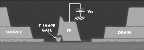
Figure 1 SEM cross-sectional photograph of the field-plate device.
After the highly selective succinic acid chemical gate recess process, 5000 Å-thick Ti/Pt/Au-gates were deposited by a lift-off process. At this stage, the Schottky layer and channel layer beneath the gate recess region were easily oxidized by moisture and generated surface states. Therefore, before the deposition of the FP metal, a 1500 Å SiNx was deposited by plasma enhanced chemical vapor deposition (PECVD) at 280°C for passivation and insulation between gate and FP metals. The 11000 Å-thick FP metal (Ti/Au =3000Å/8000Å) was then deposited on the SiNx passivation layer using an electron-beam evaporator. The FP metal extension is identical to the gate recess region because the channel is close to the surface after the recess process, so that the FP induced depletion region is used to keep the carrier far away from the surface states. Finally, a dense SiNx layer was deposited as a protection layer for improving device reliability. Figure 1 shows the SEM cross-sectional view photograph of the field-plate device.

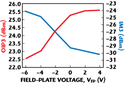
Figure 2 IM3 and OIP3 vs. VFP of an FP device at 5.2 GHz.
A fabricated 0.15 μm-long gate PHEMT with a 2.15 μm-long FP metal was tested on-wafer and the microwave power characteristics were evaluated by a load-pull system with automatic tuners, which provides conjugate-matched input and load impedances simultaneously for maximum output power. The microwave load-pull power performance was conducted at 5.2 GHz under a drain bias of 3 V, with various VFP. The field-plate voltages were supplied by a single DC probe with its ground connected with the device source terminal to guarantee the exact field-plate biases. The gate bias was chosen for a Class AB operation. The output power density degraded, following the trends of Ids at various VFP. However, this is not the case for the device linearity characteristics. The third-order inter-modulation (IM3) product from the device output spectra versus the input RF power, which is an important index of the device linearity, was determined by injecting two-tone frequencies, 5.200 GHz (f1) and 5.201 GHz (f2). These two adjacent signals generated IM3 output power (2f1 - f2 and 2f2 - f1) owing to device intrinsic nonlinearity. Figure 2 shows the measured third-order output intercept points (OIP3) as a function of VFP for a single device.

Figure 3 Gate leakage current for an FP device and a standard device under identical drain current.
The OIP3 was determined by extracting the curves intersection point of fundamental and IM3 output versus input power. The OIP3 is 22.8 dBm at a VFP of +4 V operation and 25.5 dBm at a VFP of -6 V operation. Furthermore, the IM3 output power of the device with a VFP of -6 V (-30.5 dBm) outperforms the device with a VFP of +4 V (-23.9 dBm) at an input power of -10 dBm. The device performed at a lower output power density at negative VFP, which results in a small dynamic range. However, there are two mechanisms to explain the IM3 improvement at a negative VFP operation. First of all, the gate leakage current (Ig) of a field-plate device with a negative VFP is lower than a standard one. Figure 3 compares the gate leakage current characteristics between a fabricated field-plate device and a standard device under identical drain current (Id). Based on a previous investigation,8 the higher Ig will generate extra harmonics power and degrade the device linearity.
For the observation of the gate leakage current dependence of VFP in the field-plate structure, the gate leakage current was measured at a bias VFP = -4 V. The measured gate leakage current level for this case is 3.9 mA at Pin = 10 dBm, which is 17 percent lower than the reference case of a standard device. This gate leakage current improvement can lead to an increasing of breakdown voltage. Secondly, the carrier transportation path between drain and terminals was suppressed to a deeper channel at a negative VFP and the carriers were kept away from the surface traps, which resulted in small harmonic power and lower DC-RF dispersion. The tunable field-plate voltage technique can effectively adjust the device power and linearity performance in a single device. On the other hand, when developing a high-power amplifier module, the tunable VFP can be applied to select various output power density and optimize their linearity instead of the complicated PHEMT epitaxial structure modification and process-related regulation (the depth or width of the gate recess region). Therefore, this technique exhibits a high potential for retrenching the fine-tuned procedure of the commercial microwave circuit modules without extra DC consumption.

Figure 4 Cgd and gmi vs. VFP.
The on-wafer microwave S-parameters evaluation of a Wg = 150 μm device was carried out in a common-source configuration with an Agilent E8364B PNA network analyzer from 0.05 to 40 GHz. By extracting the equivalent circuit model from the device S-parameters at various VFP, both the gate-to-drain capacitance (Cgd) and intrinsic transconductance (gmi) increased with VFP, as shown in Figure 4. However, the gate-to-source capacitance (Cgs) was almost identical (~400 fF) at different VFP. Cgd and Cds were strongly influenced by the thickness of the FP-induced depletion region, which is controlled by VFP; this phenomenon also shows the same trend with DC measurement results. Based on the Cgs measured results, the gate-to-source depletion region, which is the most important factor to determine the device microwave performance, was less influenced by VFP. In other words, the tunable FP voltage technology can adjust and modulate the device DC and RF characteristics with less sacrifice to the device gain-bandwidth product. Besides, the intrinsic gm also increased from 53 to 62 mS, which is attributed to the drain current improvement from VFP = -10 V to VFP = +4 V.

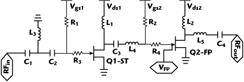
Figure 5 Circuit topology of the proposed FP driver amplifier.
According to a previous study,7 using a nonlinear current method, a Volterra model is extracted from a standard GaN HEMT to predict third-order intermodulation distortion (IMD3), highlighting various distortion mechanisms, by which the dominant distortion behavior is efficiently localized. The simulation results proved that the third-order nonlinearity, arising from the gate-drain feedback capacitance Cgd, has a major influence on the total lower third-order intermodulation distortion (IMD3L). Besides the previous observation of developing an FP structure, by which the increasing of Cgd was seen through simulation by scaling Cgd to 150 percent, the device linearity was improved by approximately 3 dB. Therefore, it can be concluded that this technology is especially attractive for high-linearity RF circuits with advantages of ease to apply and adjust a moderate VFP bias, no extra DC consumption, and based on a standard fabrication process.9

Figure 6 Photograph of the proposed FP driver amplifier.
Driver Amplifier Design and Measured Results
A 5.2 GHz driver amplifier was demonstrated using a 0.15 μm gate length depletion-mode PHEMT process, using the tunable field-plate bias voltage technology. The FP driver amplifier circuit diagram and the corresponding photograph of the fabricated MMIC for the completed amplifier are shown in Figures 5 and 6, respectively. The chip dimensions of the MMIC are 1.5 × 1 mm. A standard driver amplifier was also fabricated for power performance comparison, under the identical design approach as the FP one with the same size. The difference between these two amplifiers was the selection of a standard device or a FP device in the output stage. Figure 7 shows the corresponding photograph of the standard driver amplifier. For both designs, the gate biases were chosen for a Class AB operation with a current of 35 mA for the first stage and a current of 47 mA for the output stage, which is a compromise by considering device output power (Pout).

Figure 7 Photograph of the standard driver amplifier.
The PA is power matched at the output matching network, which is designed to transfer maximum output power from the FET to a 50 Ω system. According to the Cripps technique, the required optimized large-signal load impedance Zopt,Q2 is composed of Ropt,Q2 and Cds,Q2. The output power matching network was designed to transfer the Zopt,Q2 to 50 Ω, which comprised a series spiral inductance and a series blocking capacitance. The inter-stage matching network was designed to transfer GammaIN,2 to the Zopt,Q1 in order to minimize the mismatch loss. A gate resistor is used in each stage in order to achieve a lossy match and to improve circuit stability. The circuit stability is then further confirmed by the simulation of the stability factor. Finally, the input network was designed to smooth the small-signal gain and to improve the impedance match for a better input return loss.

Figure 8 Measured S-parameters of the proposed FP driver amplifier.
While considering the FP device power density degrading in terms of trends of Ids with the decreasing field-plate voltage VFP at the output stage, the gate bias of an FP device should be set a little higher to generate identical power density with respect to a standard device. By adjusting the gate bias of the FP device at the output stage with a difference of 0.05 V slightly higher than the standard device, the output current level and DC transconductance could be ensured as high as the standard one.
Under the bias conditions of Vds1 = Vds2 = 3 V, Vgs1 = -0.5 V, Vgs2 = -0.45 V and VFP = -4 V, the small-signal gain of the field-plate driver amplifier was measured as 31 dB at 5.2 GHz (see Figure 8). The standard driver amplifier showed a 32 dB small-signal gain under the bias conditions of Vds1= Vds2= 3 V, Vgs1= Vgs2=-0.5 V.

Figure 9 Comparison between output power and gain of an FD and standard driver amplifier.

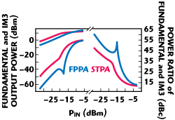
Figure 10 Two-tone measurements with 5.200 and 5.201 GHz fundamental frequencies and IM3 vs. input power for standard and FP driver amplifiers.
Under identical power consumption, the comparisons between a standard and a field-plate amplifier in output power and associated power gain as a function of input power at 5.2 GHz, are shown in Figure 9. The 1 dB gain compression power (P1dB) of the FP amplifier was 15.1 dBm with respect to the standard one of 14.2 dBm. The maximum output power of the FP amplifier was 17.8 dBm with respect to the standard one of 17 dBm. The two-tone evaluation was conducted with frequencies of 5.200 and 5.201 GHz and the results are shown in Figure 10. The power ratios between fundamental and IM3 products of the FP driver amplifier and the standard driver amplifier are 43.4 dBc for the FP device and 35.3 dBc for the standard device at an input power of -20 dBm. The IM3 output powers are -40.2 and -28 dBm for FP device and standard device, respectively. The measured input power at the third-order intercept point (IIP3) is -2 dBm for the FP amplifier; this value is -4 dBm for the standard amplifier. From the above experimental results, it is concluded that an adjustable circuit output power and linearity approach of a driver amplifier design by using a simple tunable field-plate voltage technique has been developed successfully. This approach is easily realized to suppress the harmonic powers by appropriate VFP bias point selection and no extra DC consumption is required, which is attractive for high-linearity amplifier design.
Conclusion
Linearity performance improvement of a large-signal AlGaAs/InGaAs PHEMT was demonstrated by implementation of a field-plate structure. The benefit of an FP structure, which increases the feedback gate-to-drain capacitance, dominates the improvement in device linearity. By applying a negative bias on the field-plate metal, the FP-induced surface depletion region is thicker and the carriers between drain and gate terminals are removed from the surface, which reduces the leakage current. Therefore, the device DC-to-RF dispersion and the linearity of the PHEMT can also be improved by this factor. Through the moderate bias point selection of VFP, the field-plate technology has also been demonstrated in a 5.2 GHz driver amplifier. When compared with a standard driver amplifier, it showed great promise for circuit linearity improvement.
Acknowledgment
The authors are grateful to WIN Semiconductors Corp. for device fabrication. This work is financially supported by the National Science Council (NSC-97-2221-E-182-048-MY3) and the Green Technology Research Center of Chang Gung University, Taiwan, ROC.
References
- S. Yunju and L.F. Eastman, "Large-signal Performance of Deep Sub-micrometer AlGaN/AlN/GaN HEMTs with a Field-modulating Plate," IEEE Transactions on Electron Devices, Vol. 52, No. 8, August 2005, pp. 1689-1692.
- A. Chini, D. Buttari, R. Coffie, L. Shen, S. Heikman, A. Chakraborty, S. Keller and U.K. Mishra, "Power and Linearity Characteristics of Field-plated Recessed-gate AlGaN-GaN HEMTs, " IEEE Electron Device Letters, Vol. 25, No. 5, May 2004, pp. 229-231.
- X. Huili, Y. Dora, A. Chini, S. Heikman, S. Keller and U.K. Mishra, "High Breakdown Voltage AlGaN-GaN HEMTs Achieved by Multiple Field Plates," IEEE Electron Device Letters, Vol. 25, No. 4, April 2004, pp. 161-163.
- Y. Nakasha, M. Nagahara, Y. Tateno, H. Takahashi, T. Igarashi, K.Joshin, J. Fukaja and M. Takikawa, "A Low-distortion High-efficiency E-mode GaAs Power FET Based on a New Method to Improve Device Linearity Focused on gm Value," IEDM Technical Digest, December 1999, pp. 405-408.
- A. Chini, D. Buttari, R. Coffie, L. Shen, S. Heikman, S. Keller and U.K. Mishra. "Effect of Gate Recessing on Linearity Characteristics of AlGaN-GaN HEMTs," Proceedings of the 2004 Device Research Conference.
- Y.F. Wu, M. Moore, T. Wisleder, P.M. Chavarkar, U.K. Mishra and P. Parikh, "High-gain Microwave GaN HEMTs with Source-terminated Field-plates," 2004 IEEE International Electron Devices Meeting Digest, pp. 1078-1079.
- E.R. Srinidhi, A. Jarndal and G. Kompa, "A New Method for Identification and Minimization of Distortion Sources in GaN HEMT Devices Based on Volterra Series Analysis," IEEE Electron Device Letters, Vol. 28, No. 5, May 2007, pp. 343-345.
- H.C. Chiu, S.C. Yang, F.T. Chien and Y.J. Chan, "Improved Device Linearity of AlGaAs/InGaAs HFETs by a Second Mesa Etching," IEEE Electron Device Letters, Vol. 23, No. 1, January 2002, pp. 1-3.
- H.C. Chiu, C.S. Cheng, S.W. Lin and C.C. Wei, "High-linearity SPDT Pseudomorphic HEMT Switch Based on Tunable Field-plate Voltage Technology," IEEE Transactions on Electron Devices, Vol. 56, No. 4, April 2009, pp. 541-545.
