The size of the antenna for a given application does not depend purely on the technology, but on the laws of physics where the antenna size with respect to the wavelength has the predominant influence on the radiation characteristics. With modern day communication devices becoming smaller and lighter, demand for low-profile antenna designs is greater than ever.1
One way of realizing a low-profile antenna design is to use a high impedance ground plane in place of the conventional metallic ground plane.2-7 Metallic plates are used as ground planes to redirect the back radiation and provide shielding to the antennas. By nature, the conventional ground planes that are perfect electric conductors (PEC) exhibit the property of phase reversal of the incident currents that result in destructive interference of both the original antenna currents and the image currents. To overcome this effect, antennas are to be placed at a quarter wavelength above the metallic ground plane, making the size of the antenna bulky at low frequencies. To reduce the size of the antenna, a ground plane that is a dual of the conventional PECs is needed; in other words, a perfect magnetic conductor (PMC) is required. But how can a PMC that is not available in nature be realized? The answer to this problem is provided in the form of high impedance surfaces (HIS), which can essentially be considered as artificial magnetic conductors.8,9
HISs are popular for their widespread applications in reflect array antennas, low-profile antennas, electromagnetic absorbers and polarizers.10-13 These surfaces exhibit unique properties like the in-phase reflection of incident waves and the suppression of surface waves. Different antenna parameters such as gain, impedance and size can be enhanced by incorporating the HISs into the antenna structures. The design of the HISs can be optimized to tailor their electromagnetic properties depending on the operational requirements. Computer-aided design tools have enabled the solution of complex problems by means of numerical optimization algorithms.14,15 A large number of optimization methods are presently available for solving electromagnetic problems. Deciding the most appropriate method for a given problem, however, is a non-trivial task and depends on factors like the number and range of the varying parameters, the goal of the optimization, the model size and the resources available.
Two-dimensional (2D) arrays of periodic resonant elements (printed or complementary slot) interact with electromagnetic waves within certain frequency band(s) and can be characterized as frequency selective surfaces (FSS). Different FSS elements have been described in the literature, where each design has its own advantage over the other. The multiband dipole structures are polarization dependent, the symmetric designs are dual-polarized and the fractal structures are compact designs. The HIS is realized by printing the periodic array of FSSs over a metal-backed dielectric substrate. It is important to optimize the performance of HIS over the frequencies of interest. It is observed that the characteristics of the FSS and HIS follow each other. This correlation can be exploited to speed up the optimization process by carrying out the design in two steps:
- Optimize the free-standing FSS
- Realize the HIS by printing the optimized FSS on a metal-backed dielectric substrate

Figure 1 The FSS unit cell.
Even though there is growing demand for wideband antennas, a narrowband design has its advantages in cordless and wireless phone applications that operate at 49 MHz, 900 MHz, 2.4 GHz and 5.8 GHz. Interference from adjacent frequency bands can be avoided by using narrowband antennas that operate only around the frequency of interest. This article describes a novel FSS structure that is optimized for steep behavior of the reflection coefficient. The FSS unit cell is the combination of a Jerusalem cross and a three-step fractal patch, as shown in Figure 1. The reflection characteristics of the FSS structure are explored in designing a HIS that can be used as a potential substrate for antennas in cordless phone applications to reduce cross talk. The performance of the HIS substrate is demonstrated with a 5.8 GHz low-profile monopole (quarter wavelength) antenna with a 0.07 dielectric thickness. The monopole is first analyzed as a wire structure; this design is then translated to a printed format.
FSS Design and Optimization

Figure 2 Reflection coefficient of a periodic array of unit cells.
The operation of the FSS structure depends on the resonance of the unit cell. A periodic array of the unit cell interacts with the electromagnetic wave and resonates at certain frequencies, where it acts as a band stop filter with total reflection of the incident plane wave, as shown in Figure 2.
The initial design of the FSS structure with broadband characteristics is optimized for sharp narrow band characteristics. The commercial software FEKO22 is used for the analysis of the FSS structure using two different optimization methods: Simplex Nelder-Mead and Particle Swarm Optimization (PSO).20
Simplex (Nelder-Mead Method)
The Simplex Nelder-Mead algorithm is a local or hill climbing algorithm in which the final optimum relies strongly on the starting point. The term simplex refers to the geometric figure formed by a set of N+1 points in an N-dimensional space. The basic idea of the simplex method is the comparison of values of the combined optimization goals at the N+1 points of the general simplex (where each point represents a single set of parameter values) to facilitate the movement of the simplex towards the optimum point during an iterative process. The movement of the simplex is achieved using three operations: reflection, expansion and contraction.
Particle Swarm Optimization (PSO)
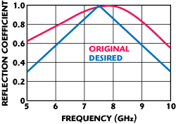
Figure 3 FSS reflectivity behavior, original and desired goal.
Particle Swarm Optimization is a global search algorithm, which is a population-based stochastic evolutionary computation technique based on the movement and intelligence of swarms found in nature. The mechanism of PSO can be best described using the analogy of a swarm of bees in a field, whose goal is to find the highest concentration of flowers where each bee represents a set of parameter values. Every bee has information about the position of flower abundance based on its own experience (local best) and the position of maximum flower abundance based on the experience of all the other bees (global best). Based on the weights given to individuality or peer pressure, a bee flies in a direction between the positions of the local and the global bests. Once the flying is done, the bee conveys the new found information to all the other bees, which then adjust their positions and velocities. With this constant exploring and exchange of information, all the bees are eventually drawn towards the position of the highest concentration of flowers. The possible optimization parameters/variables in the proposed FSS unit cell are the dimensions of the Jerusalem cross arms and the fractal patch. An optimization mask was used to specify the optimization goal, as shown in Figure 3.
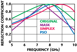
Figure 4 Comparison of Simplex and PSO algorithms.
Being a local optimizer, the convergence of the Simplex algorithm is much faster compared to the global optimizer PSO. However, unlike the global optimizer PSO, the success of the Simplex depends on the starting point, which carries the disadvantage of converging to a local minimum. From Figure 4, it is clear that the global optimizer PSO was able to approximate the mask more closely compared to the Simplex, but at the cost of a huge run time.

Figure 5 Comparison between PSO and Simplex-PSO hybrid optimization.
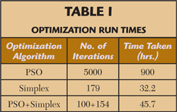
To improve the chances of reaching the global minimum without compromising on the speed of convergence, PSO is hybridized with Simplex, where the global optimizer will be used to find the starting point for the local optimizer. The hybridized method has improved the speed of the optimizer without compromising on the ability to reach the global goal. In this process, the local optimizer was started after 100 iterations of the global optimizer. The local optimizer Simplex converged to the global minimum in 154 iterations, as shown in Figure 5, reducing the runtime by 95 percent. Table 1 describes the number of iterations and the time taken for each optimization algorithm to converge on a 2 GHz, EM64T Linux machine that has 2 physical CPUs with 4 cores per CPU.
HIS Design and Validation
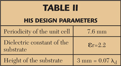
The optimization completes the first step in the realization of the artificial magnetic conductor, taking the design process to the next stage, where the optimized FSS structure is printed on a metal-backed dielectric substrate. The design parameters of the HIS shown in Figure 6 are given in Table 2, where λd denotes the wavelength inside the dielectric at 5.8 GHz.

Figure 6 HIS realized with optimized FSS.
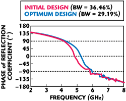
Figure 7 Reflectivity characteristics of HIS realized with un-optimized and optimized FSS.
The reflectivity characteristics of the HIS ground planes realized using the un-optimized and the optimized FSS structures reveals the correlation between the FSS and the HIS. The HIS realized with optimized FSS reduced the bandwidth of the un-optimized design by 7 percent, as shown Figure 7, where the bandwidth is defined for the phase of the reflection coefficient varying between +90° and -90°.
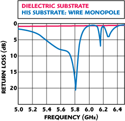
Figure 8 Return loss of monopole on HIS and dialectric substrate.
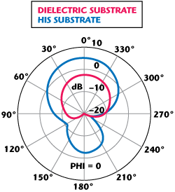
Figure 9 Monopole antenna gain on HIS and dialectric substrate at 5.8 GHz.
Unlike the conventional PEC ground planes, antennas can be placed very close to the surface of the HIS ground plane resulting in a low-profile design.21 The performance of the low-profile design is tested with a quarter wave (at cordless frequency of 5.8 GHz) monopole antenna with the HIS ground plane and a metal-backed dielectric substrate of same thickness. Figures 8 and 9 validate the performance of the HIS ground plane with low return loss and an improvement of 7.5 dB in the gain over the metal-backed dielectric substrate.
Planar Antenna

Figure 10 Printed monopole antenna with the HIS between the substrate layers.
Antennas are generally preferred in a printed format, so that they can be made flush with the surrounding environment. Printed planar antennas also have the advantage of being cheap and more convenient to manufacture and lend themselves more easily to mass production than non-printed antennas. For these reasons the design is transferred from the protruding cylindrical monopole structure to one involving a planar printed monopole. The wire monopole (modeled as a cylinder) is transformed to the printed monopole using the well known formula α=0.25w, where 'a' is the radius of the cylinder and 'w' is the width of the strip. This strip monopole is located at the same height as the axis of the cylindrical monopole to keep the electromagnetic relationship between the High Impedance Surface (HIS) and the monopole intact. It is not desirable that the gap between the strip monopole and the top surface be left as free-space as this leaves the monopole vulnerable to damage and also defeats the purpose of ease of manufacture. In order to avoid these problems this space is filled with a dielectric superstrate (relative to the HIS) that has the same dielectric properties as the substrate. Figure 10 shows the printed monopole antenna on top of the newly added dielectric layer. The HIS is located at the boundary of the dielectric layers and can be seen in the wire frame view. A TEM mode is excited from the end of a coaxial cable, whose outer conductor terminates at the ground plane and inner conductor extends further through the substrate to excite one end of the monopole.
Replacing the air layer with a dielectric substrate alters the electrical length of both the monopole and the HIS, thereby moving the resonant frequency away from the desired value of 5.8 GHz. To re-tune the antenna back to 5.8 GHz, the monopole is scaled by a factor of
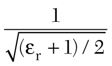
and the HIS by a factor of
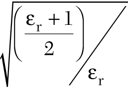
It should be pointed out that although the scaling brings the resonance very close to 5.8 GHz, some finer adjustments of these factors is required to make the resonance fall exactly at 5.8 GHz. Figure 11 compares the S11 of the planar design with the previous non-planar design and the non-HIS substrate. From the graph, note that the planar design leads to an increase in the return loss bandwidth (defined as being lower than 10 dB). Due to the improved impedance match at the center frequency, the gain of the antenna is increased from a value of 5.35 dB (non-planar monopole) to a value of 7.73 dB (planar monopole). Figure 12 illustrates this behavior and shows the gain pattern in the elevation plane (XZ).
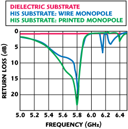
Figure 11 Comparison of the return loss.

Figure 12 Monopole antenna gain for the planar and non-planar antennas at 5.8 GHz.
Effect of the Substrate Length and Width

Figure 13 Effect of reducing the substrate size.
As the overall size of the antenna, including the HIS ground plane, is important for use in compact mobile devices, the effect of the substrate length and width on the impedance characteristics of the antenna was studied. Figure 13 shows the variation in return loss due to a decrease in substrate size. It can be seen that decrease in substrate size narrows the impedance bandwidth. Substrate size can be used to control the impedance bandwidth.
Conclusion
A novel FSS structure is designed by combining the fractal and Jerusalem cross elements. The resultant structure provides more flexibility in controlling the reflection coefficient behavior. The efficiency of the optimizers can be increased by hybridizing the local optimizer with the global optimizer, which is demonstrated in the case of the proposed FSS structure. The narrowband HIS realized from the optimized FSS can be used in designing low-profile antennas. The low-profile monopole antenna on the HIS ground plane with a substrate thickness of 0.07 λd improves the gain of the antenna by 7.5 dB. Further improvement to the antenna can be made by transforming the design into a planar antenna, which increases the gain from 5.35 to 7.73 dB. It is found that doing so increases the return loss bandwidth of the antenna. A study of the substrate size shows that a reduction in size causes the antenna to become narrow band, but at the cost of the resonance null depth.
References
- A.K. Skrivervik, J.F. Zurcher, O. Staub and J.R. Mosig, "PCS Antenna Design: The Challenge of Miniaturization," IEEE Antennas and Propagation Magazine, Vol. 43, No. 4, August 2001, pp. 12-27.
- D. Sievenpiper, R. Broas and E. Yablonovitch, "Antennas on High-impedance Ground Planes," 1999 IEEE MTTS International Microwave Symposium Digest, Vol. 3, pp. 1245-1248.
- M.E. Ermutlu, C.R. Simovski, M.K. Karkkainen, P. Ikonen, A.A. Sochava and S.A. Tretyakov, "Patch Antennas with New Artificial Magnetic Layers," arXiv:physics/0504075v1, April 2005.
- A.P. Feresidis, G. Goussetis, S. Wang and J.C. Vardaxoglou, "Artificial Magnetic Conductor Surfaces and Their Application to Low-profile, High-gain Planar Antennas," IEEE Transactions on Antennas and Propagation, Vol. 53, No. 1, January 2005, pp. 209-215.
- F. Yang, Y. Rahmat-Samii and A. Kishk, "Low-profile Patch-fed Surface Wave Antenna with a Monopole-like Radiation Pattern," IET Microwave Antennas and Propagation, Vol. 1, No. 1, February 2007, pp. 261-266.
- L. Schreider, X. Begaud, M. Soiron, B. Perpere and C. Renard, "Broadband Archimedean Spiral Antenna Above a Loaded Electromagnetic Bandgap Substrate," IET Microwave Antennas and Propagation, Vol. 1, No. 1, February 2007, pp. 212-216.
- A. Erentok, P.L. Luljak and R.W. Ziolkowski, "Characterization of a Volumetric Metamaterial Realization of an Artificial Magnetic Conductor for Antenna Applications," IEEE Transactions on Antennas and Propagation, Vol. 53, No. 1, January 2005, pp. 160-172.
- C.R. Simovski, M.E. Ermutlu, A.A. Sochava and S.A. Tretyakov, "Magnetic Properties of Novel High Impedance Surfaces," IET Microwave Antennas and Propagation, Vol. 1, No. 1, February 2007, pp. 190-197.
- D.J. Kern, D.H. Werner, A. Monorchio, L. Lanuzza and M.J. Wilhelm, "The Design Synthesis of Multiband Artificial Magnetic Conductors Using High Impedance Frequency Selective Surfaces," IEEE Transactions on Antennas and Propagation, Vol. 53, No. 1, January 2005, pp. 8-17.
- P. Ratajczak, J.M. Baracco and P. Brachat, "Adjustable High Impedance Surface for Active Reflectarray Applications," 2007 European Conference on Antennas and Propagation Proceedings, pp. 1-6.
- F. Yang and Y. Rahmat-Samii, "Reflection Phase Characteristics of the EBG Ground Plane for Low Profile Wire Antenna Applications," IEEE Transactions on Antennas and Propagation, Vol. 51, No. 10, October 2003, pp. 2691-2703.
- V.V.S. Prakash and R. Mittra, "Analysis of Interaction Between Microwave Antennas and Frequency Selective Surface (FSS) Radomes," 2003 IEEE Antennas and Propagation Society International Symposium Digest, Vol. 4, pp. 404-407.
- G.I. Kiani, A.R. Wiley, P. Karu and Esselle, "Frequency Selective Surface Absorber Using Resistive Cross-dipoles," 2006 IEEE Antennas and Propagation Society International Symposium Digest, pp. 4199-4202.
- S. Genovesi, R. Mittra, A. Monorchio and G. Manara, "Particle Swarm Optimization for the Design of Frequency Selective Surfaces," IEEE Antennas and Propagation Letters, Vol. 5, No. 1, December 2006, pp. 277-279.
- M. Ohira, H. Deguchi, M. Tsuji and H. Shigesawa, "A Singular Characteristic of Single-layer Frequency Selective Surface with the Element Optimized by GA," 2003 IEEE Topical Conference on Wireless Communication Technology Digest, pp. 216-217.
- M. Hiranandani, A.B. Yakovlev and A.A. Kishk, "Artificial Magnetic Conductors Realized by Frequency Selective Surfaces on a Grounded Dielectric Slab for Antenna Applications," IEEE Proceedings - Microwave Antennas and Propagation (Part H), Vol. 153, No. 5, October 2006, pp. 487-493.
- C.R. Simovski, P. de Maagt and I.V. Melchakova, "High-impedance Surfaces Having Stable Resonance with Respect to Polarization and Incidence Angle," IEEE Transactions on Antennas and Propagation, Vol. 53, No. 3, March 2005, pp. 908-914.
- Y. Zhang, J. von Hagen, M. Younis, C. Fischer and W. Weisbeck, "Planar Artificial Magnetic Conductors and Patch Antennas," IEEE Transactions on Antennas and Propagation, Vol. 51, No. 10, October 2003, pp. 2704-2712.
- G. Goussetis, Y. Guo, A. P. Feresidis and J.C. Vardaxoglou, "Miniaturized and Multiband Artificial Magnetic Conductors and Electromagnetic Band Gap Surfaces," 2004 IEEE Antennas and Propagation Society International Symposium Digest, Vol. 1, pp. 293-296.
- M. Schoeman, U. Jakobas and B. Woods, "FEKO Optimization Capabilities: Simplex, Particle Swarm, Genetic Algorithm," 2008 ACES International Conference, pp. 281-286.
- G. Gampala, "Analysis and Design of Artificial Magnetic Conductors for X-band Antenna Applications," Master's thesis, University of Mississippi, 2007.
- FEKO Suite 5.4, EM Software and Systems (www.feko.info), 2008.
Gopinath Gampala received his bachelor's degree in electronics and communications engineering from Jawaharlal Nehru Technological University, Hyderabad, India, in 2005, and his master's degree in electrical engineering from the University of Mississippi in 2007. He joined EM Software & Systems USA Inc. in 2008, where he is currently working as an applications engineer.
Rohit Sammeta received his bachelor's degree in electrical engineering from IIT-Bombay, India, in 2004, and his master's degree from the University of Mississippi in 2007. He joined EMSS USA Inc. as an applications engineer where he provides advanced technical and modeling support for FEKO, an industry leader in EM simulation software. He is also engaged in and responsible for exploring and expanding FEKO's frontiers of applications, while simultaneously performing research in basic electromagnetics.
C.J. Reddy received his B.Tech. degree in electronics and communications engineering from Regional Engineering College (now the National Institute of Technology), Warangal, India, in 1983. He received his M.Tech. degree in microwave and optical communication engineering and his PhD degree in electrical engineering, both from the Indian Institute of Technology, Kharagpur, India, in 1986 and 1988, respectively. He is currently the President and Chief Technical Officer of Applied EM Inc., a small company specializing in computational electromagnetics, antenna design and development.
