In the 1980s, the running joke was "GaAs is the future and always will be." Up until that time it had shown great promise, but was having a hard time living up to its performance potential and was plagued by high material costs and inconsistent processes. However, due to large investments by the government/military (mostly the DARPA MIMIC programs) in the 1980s and high commercial demand for wireless applications in the 1990s (such as satellite TV and cellular handsets), it has become the mainstay of the RF/microwave industry for the last couple of decades. Many companies built large GaAs fabs in the '80s and '90s, but today most rely either totally or partially on foundries for their supply of chips. This allows for greater flexibility in fast changing markets and many "fabless" companies have leveraged this business model to develop lower fixed cost businesses that have flourished over the last ten years.
Squeeze Play
Today, GaAs is being squeezed more than ever by competing Si technologies and newer high voltage compound semiconductor materials like GaN and SiC. Recent developments in Si CMOS and BiCMOS processes have achieved cut-off frequencies over 300 GHz,1 allowing it to compete in many applications where GaAs had mostly dominated. Si chips have a large cost advantage in high volumes and offer superior digital integration opportunities for single chips solutions (BiCMOS). In addition, LDMOS processes have significantly advanced with higher voltage designs that produce robust transistors capable of output power performance as good as GaN and SiC, but at a much lower cost. There is also competition from UltraCMOSTM (Peregrine Semiconductor) for lower power, fast switching applications. They are now expanding the process with several other types of devices to further compete with GaAs. SiGe processes are creating highly integrated single chip solutions at high frequencies such as automotive radar at 24 and 77 GHz and point-to-point radios. There are a large number of RF Si foundries that have high capacities available such as Taiwan Semiconductor (TSMC), Tower/JAZZ Semiconductor, IHP Microelectronics, IBM, austriamicrosystems, etc., so the costs for large volumes are relatively low with available capacity.

As Si technologies mostly squeeze GaAs from the lower frequency and lower power applications side, other compound semiconductors such as GaN and SiC are squeezing GaAs from the high frequency, high power side where it has always excelled. As with GaAs in the 1980s, these other compound semiconductor technologies are benefiting from government/military funding and the commercial demand for more efficient "green" technologies. GaN (typically grown on Si or SiC substrates) has a wider band gap (higher breakdown voltages of 100 V or more) and higher gain, which means it has an advantage in high power applications. Although most GaN development is in high power applications, it also shows good low noise properties giving it the ability to produce LNAs that can withstand higher input voltages in the receive chain. This will enable multi-function LNA/switch MMIC devices in addition to high power amplifiers. Table 12 shows a comparison of material properties for various semiconductor materials.
Higher gain GaN devices are starting to make a significant impact in military programs and cellular infrastructure applications; GaN can achieve 5 W/mm or more compared to GaAs, which has about 1 W/mm (some special high voltage GaAs processes can reach about 1.5 W/mm). With all that heat being created from these high power devices, the packaging costs can be relatively high and swing back in favor of GaAs. GaAs also typically has higher linearity than other semiconductor type devices, which can be a big advantage in the newer 3G/4G systems that require high linearity for OFDM. RFMD recently announced the opening of its GaN fabrication facility for foundry business to join others such as TriQuint, United Monolithic Semiconductors (UMS), Eudyna/Fijitsu, Cree and Nitronex. Most GaAs foundries plan to start offering GaN services this year if they have not already announced it.
Another high voltage compound semiconductor material, SiC, has demonstrated impressive high-power devices for lower frequency, pulsed applications from companies like Microsemi. These devices also have much higher breakdown voltages than GaAs and superior thermal conductivity properties. However, the wafer sizes are smaller and are much more expensive than some competing technologies. So far SiC has been competing in the relatively lower frequency ranges for pulsed applications.
Cost and Performance
GaAs has fought back on both the cost and performance side of the battle. GaAs foundry wafers cost up to $2500 a wafer versus a Si CMOS wafer of about $1000 and a SiGe wafer of about $2500; however, both Si processes are on larger 8 inch wafers compared to 6 inch GaAs wafers so they yield about twice as many die.3 Therefore, the chip cost is far less for Si-based processes including the more specialized SiGe processes based on volume.
However, there are two other cost factors that can make GaAs less expensive. First, GaAs mask sets typically cost from about $25 to $50k versus Si-based processes that cost from about $50 to $300k3 so the initial investment is larger. Second, about 95 percent of RF cellular handset front-end devices are done by Integrated Device Manufacturers (IDM), whose internal costs are far less because they own their own fabs.3 The internal wafer for IDMs is about the same as a Si CMOS foundry wafer so they are competitive with Si if produced for internal use. Therefore, looking at the total cost, lower to medium volume applications will probably be cheaper on GaAs while high volume applications (tens or millions or more) will be cheaper on Si-based technologies. One possible exception in the market today is millimeter-wave radios/automotive radar applications where SiGe single chip solutions have been custom developed to leverage high levels of integration (single chip radios) and are displacing some GaAs-based solutions. NXP is an example of a company making a significant push to replace GaAs devices with SiGe products as they recently announced they are releasing 50 new products by the end of 2010 for this purpose.

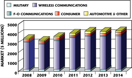
Figure 1 Projected GaAs market value by application from 2008 to 2014
GaAs Foundry Market
The GaAs market in 2008 grew 6 percent year-on-year, but really declined in the fourth quarter of that year according to Strategy Analytics. Strategy Analytics then reported the market declined by over 10 percent in 2009. However, the outlook going forward is better as they are projecting the GaAs market to be worth over $4.3 B by 2014 growing with a CAGR of 6 percent. Figure 14 shows the GaAs market size for the major application areas with wireless communications being the primary growth market. The dominant market within wireless communications is for handset applications for front-end modules in the cellular market.

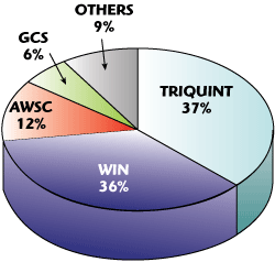
Figure 2 GaAs market share by company5
The current total market size data from Strategy Analytics for the GaAs foundry business is about $360 M with TriQuint and WIN Semiconductor neck-in-neck with a market share of a little over a third each (see Figure 2).5 WIN is the largest pure play GaAs foundry and has rapidly closed the gap with the market leader TriQuint over the past couple of years.
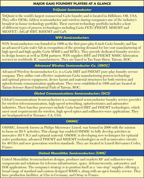
These two market share leaders are followed by Advanced Wireless Semiconductor Co. (AWSC) and Global Communication Semiconductors (GSC). United Monolithic Semiconductor (UMS) and OMMIC are the major European players that tend to concentrate on lower volume applications like defense and aerospace, so they are not major players in the overall market share data. In the 2007 time frame, several pure play GaAs foundries folded, including Knowledge On, Suntek and GCTC. WIN, ASWC and GSC are now the remaining major pure play foundries in the market.
There are many other captive GaAs fabs around the world, some of which do offer specialized foundry services. These include mostly defense companies such as Northrop Grumman, Cobham, Raytheon, BAE, etc., who will offer foundry services for specific large government programs or opportunities that utilize their design expertise and fit into their specific markets. However, they are mostly captive in the use of their fabs and not typically available for most applications. Other large captive commercial GaAs foundries include Skyworks, M/A-COM Technology Solutions, Anadigics, Avago, RFMD and Eudyna/Sumitomo.
GaAs devices first evolved from discrete implanted FETs to metal-eptiaxial-semiconductor field-effect transistor (MESFET) technology for integrated circuits (MMICs), but over the last decade, heterojunction bipolar transistors (HBT) have been used for most power amplifiers and pseudo-metamorphic high electron mobility transistors (PHEMT) for low noise and high frequency devices. These device types, in general, outperform MESFET technology, although the material costs are a little higher. Originally, only depletion-mode PHEMTs were available, but now foundries offer E/D PHEMT (enhancement/depletion mode PHEMT) devices, allowing for both types of transistors on a circuit. Logic type devices can be realized using enhancement mode FETs and depletion mode devices are typically used for other functions. This allows more capability on a single chip as digital logic, amplifiers, switches, LNAs, attenuators, mixers, passive devices, etc., can be integrated onto the same MMIC die.
Another device technology available is metamorphic high electron mobility transistor (MHEMT), which is very good for high frequency, low noise applications but are not widely available. These devices have lower breakdown voltages so they are not suitable for power devices. With excellent low noise, high frequency characteristics, they are mostly used in space-based applications and thus serve more niche type, low volume markets.

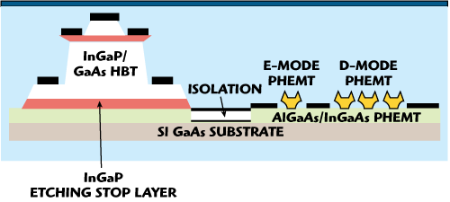
Figure 3 Cross-section diagram of WIN Semiconductor BiHEMT device structure.6
A significant trend in GaAs foundry processes over the last few years and a logical next step has been to combine both HBT and PHEMT technologies on the same MMIC so that optimal devices of all types can be realized on a single chip. This allows even more integration on a single chip while optimizing the performance of the circuit. These BiHEMT or BiFET processes (analogous to Si BiCMOS) allow HBT-based power amplifiers to be integrated next to PHEMT logic circuitry, switches and LNAs. TriQuint and WIN Semiconductor started releasing these processes in 2007. Taking a different approach than some other manufacturers who grow the FET within the emitter or collector structure, TriQuint and WIN both grow the epi layer by MOCVD on semi-insulating GaAs using a stacked layer structure with the InGaP HBT on top of the PHEMT (see Figure 3).6 In this architecture, the HBT device is processed and then the rest of the remaining HBT material is etched away to expose the PHEMT layers that are then processed. Etch stops are used between layers and the HBT device structures are isolated from the PHEMT devices for optimal performance. This structure is suitable for high-volume, low-cost manufacturing and is a good trade off with manufacturability and performance. Some other manufacturers grow the PHEMT layers within or under the HBT structures, which might simplify the epi structure but degrades the FET performance to some degree. Table 2 shows the various processes offered by the major GaAs foundries as we surveyed the six major players.

Foundry Services
Customer service and support are major factors when considering which foundry to work with. Items to consider range from design support to capacity, through-put and prototype turn-around. Most foundries provide various supporting services such as design assistance, modeling, packaging and testing. They have design libraries and models that can be accessed for designing circuits and devices, which can typically be found on their web sites. Most foundries also support several design and layout tools, as shown in Table 3.

We surveyed the major players and found the typical lead times for most GaAs foundries is 6 to 8 weeks with some longer times for more customized or complicated circuits. WIN quoted the shortest lead times of 23 to 48 calendar days. Most major foundries use 6 inch wafer lines for higher volume processes, but many 4 inch lines are still running and make sense for lower volume processes. Typical capacities range from a couple hundred to a couple thousand wafers per month.
Some of the unique features that specific foundries offer include TriQuint's vertical PIN (VPIN) diode, MHEMT, BiHEMT and GaN on SiC processes; WIN Semiconductor's 0.1 μm PHEMT and BiHEMT processes; GCS's low phase noise VCO HBT (-105 to -110 dBc/Hz at 100 KHz offset), high speed HBT (ft up to 300 GHz) and THz Schottky diode processes; UMS's defense/space qualified processes and Schottky diode process (BES up to 200 GHz); and OMMIC's specialty high frequency processes including commercially available MHEMT processes (2.2 dB NF at 94 GHz LNA MMIC with 18 dB gain).
Ongoing III-V Developments
As Si has put more cost pressure on GaAs, another significant trend in GaAs foundry processes over the past few years has been the use of optical lithography for higher frequency millimeter-wave processes to greatly reduce wafer processing costs. Typically, small geometries (less than 0.5 microns) are difficult to image using optical lithography because of the diffraction of optical light from dimensions of that size. Instead, e-beam systems are typically used. Unfortunately, e-beam systems are much more expensive and much slower as they typically use direct write systems versus a mask stepper process. There are many processing technologies available today that can avoid the optical imaging resolution issues to form very small geometries. Shorter wavelength stepper systems and specialized photoresists stacks have overcome many of these limits. As an example, TriQuint released its optical millimeter-wave processes in 2008 with processes for 0.25, 0.15 and 0.13 micron geometries on PHEMT wafers; WIN Semiconductor has a couple of 0.25 micron PHEMT processes available (see Table 4).

Another trend is outsourcing GaAs wafer fabrication to realize greater flexibility, higher margins and faster time-to-market. While fabless companies have been doing this for years, IDMs have recently been outsourcing a portion of their business to realize similar flexibility and higher margins for larger volume applications. Companies such as Skyworks, M/A-COM Technology Solutions, Avago, Freescale, Anadigics and others have been doing more of this over the last few years to compete in the up and down semiconductor markets. This is certainly favorable for the foundries as they become more important to a wider base of companies.
The main European foundries, UMS and OMMIC, have been specialty players for the most part, especially in the high performance aerospace markets. They did not benefit from large government funding in the 1980s and '90s like most US-based foundries, so they never seemed to expand beyond their regional aerospace and defense market needs. But they are now starting to expand internationally. UMS has opened a design center in Boston, MA, and a sales office in Shanghai, China, in an effort to expand its global reach. OMMIC has traditionally excelled at high frequency, low noise applications, but is becoming more commercially aware of its markets and more efficient in its technology development efforts to compete globally.

Going forward many GaAs foundries have immediate plans to begin offering GaN devices this year if they are not already providing them. TriQuint and RFMD are major players in the GaN market along with several others who specialize in this area. Most foundries see the millimeter-wave and high linearity applications as a growth area and are developing GaAs processes optimized for these opportunities. They are also expanding their services by working with design companies to develop design kits and developing advanced services or processes such as wafer bumping, chip scale packaging, multi-project wafers and Known Good Die (KGD). KGD come from a wafer that is 100 percent tested and the reject die are marked and/or removed so only fully tested, good die are delivered to the customer.
The Battle Heats Up
Si technologies are steadily improving as they increase their operating frequencies and levels of integration. They are starting to displace GaAs in some targeted millimeter-wave applications such as automotive radar and threatening to encroach upon the mainstream handset market. New market entries, such as Javelin Semiconductor, Black Sand Technologies and RFaxis, are preparing for battle with replacement parts to GaAs front-end modules and will probably see some Si solutions start to challenge the GaAs dominance in this market. Most of the designs from these players include single chip Si solutions for applications such as handset front-ends, WiFi, Bluetooth and ZigBee. For the high volume handset front-end market today, however, GaAs is still the preferred technology and offers the best performance, proven reliability and fastest time to market. The emerging Wireless HD technologies for using short-range millimeter-wave technologies (typically 60 GHz) are single chip Si technologies as their range is limited so power levels are adequate from Si solutions (SiBeam and several of the large consumer electronics companies are involved in this technology). In addition, the millimeter-wave automotive radar systems are migrating to highly integrated SiGe solutions to meet the cost constraints to bring this technology into mainstream cars (Autoliv - formerly M/A-COM, Infineon, etc.).
GaN is being inserted into future high power military radar and communications systems so it will displace GaAs to some extent in those applications, but the design cycles are long and it will take a while for this to take effect. Although most of the GaN work is being done on power devices, expect to see some GaN LNA/switch MMICs being designed to take advantage of its low noise advantages and high breakdown voltages so limiters could be eliminated improving overall performance in the receive chain. GaN is just starting to prove its worth in cellular infrastructure applications, but will also have to fight with Si LDMOS for high power solutions.
The integration technologies of GaAs have improved with the recent BiHEMT processes to enable higher performance single die solutions for applications such as Wi-Fi and bias circuitry in handsets, so GaAs is not standing still. GaAs foundries are also reducing costs with optical lithography for smaller dimensions and continued cost efficiencies. With expected CAGR growth of 6 percent over the next five years, the GaAs market still has some legs in it and should for the next several years as it battles Si and GaN with both hands. Over this time period, however, Si and GaN technologies will take away noticeable market share in select markets such as short-range millimeter-wave and high power military applications.
References
- I. Post, et al., IEDM paper 2006, 17.7.
- Strategy Analytics, "GaAs, GaN Microelectronics Market Update 2009-2014," April 2010.
- A. Anwar, C. Taylor and S. Entwistle, "Are Silicon Technologies Posed to Displace GaAs?," CS MANTECH Conference, April 14-17, 2008, Chicago, IL.
- Strategy Analytics, derived from "GaAs Industry Forecast 2008-2013," and presented in Strategy Analytics/Microwave Journal webinar, April 2010.
- Strategy Analytics, derived from "GaAs Industry Forecast 2008-2013," August 2009, http://physicsworld.com/cws/article/news/31588.
- C.K. Lin, "WIN Joins the BiFET Brigade with H2W Foundry Process," Physics World.com, http://physicsworld.com/cws/article/news/31588, November 2007.
