This article presents the design of a 3.3 to 3.8 GHz LNA, suitable for IEEE 802.16a WiMAX customer premise equipment (CPE) and base transceiver stations (BTS), built on inexpensive FR4 copper laminate epoxy glass board material using the Agilent Technologies ATF-54143 E-pHEMT (enhancement-mode pseudomorphic high electron mobility transistor).
The high loss tangent (tan ?) and relatively variable dielectric constant (?r) of the FR4 copper laminate epoxy glass material (tan ? = 0.04, ?r = 4.6) generally limits its use to applications below 3 GHz.1 For higher frequencies, designers usually use more expensive materials such as the Rogers RO4350B glass-reinforced hydrocarbon/ceramic laminate2 with tan ? = 0.003 and ?r = 3.48. Normally, the insertion loss for the FR4 board will increase rapidly when the operating frequency goes above 3 GHz, and designing 3 GHz circuits using FR4 material is usually not recommended. When using high performance devices such as the ATF-54143, however, circuits designed on FR4 material can meet the customer’s requirements for noise figure, gain and linearity. The biggest benefit to customers is the lower cost of the FR4 material. This is a critical concern for customers’ main production. With the increasing acceptance of WiMAX as a substitute for the existing broadband wire-line infrastructure in the last mile, people are now designing and testing WiMAX CPE and BTS operating at around 3.5 GHz. Properly designed circuits on a FR4 board can help to reduce the transceiver cost. Based on theoretical analysis and ADS simulation, this article presents a successful WiMAX LNA built on a FR4 board using the ATF-54143 E-pHEMT.

Target Analysis
With a single 3.6 V supply, the E-pHEMT LNA delivers a measured 0.82 dB noise figure (NF), 12.8 dB gain, +19 dBm output power at 1 dB gain compression (P1dB), 36.7 dBm third-order output intercept point (OIP3), –20 dB input return loss (IRL) and –12 dB output return loss (ORL) at 3.5 GHz.
To arrive at a balance between noise figure, gain and linearity, the device drain source current (Ids) was chosen to be 60 mA with a 3 V drain-to-source voltage; the gate-to-source voltage was 0.59 V. According to the ATF-54143 data sheet,3 this transistor has the following typical features at 3.5 GHz: Fmin = 0.65 dB, Ga = 14.5 dB, OIP3 = +37.2 dBm, S11=0.608< 149.60 (VSWR?4.1), ?opt = 0.32<-1700.

The circuit can be simulated in both linear and nonlinear operation modes by using the Agilent EEsof Advanced Design System (ADS) software. A two-port S-parameter file in the Touchstone format was used to simulate the gain, noise figure and input/output return loss; an ADS model based on the data sheet3 was applied to simulate the bias conditions and linearity. Accurate equivalent models for the resistors, inductors, capacitors and microstrip lines are critical for exact simulation because they determine the tuning elements on the circuit board. Thus, device models from Toko and Murata are adopted to model the capacitors and inductors from these two vendors, and board properties provided by the FR4 vendor are adopted to model the microstrip lines. Figure 1 shows the circuit schematic and the corresponding ADS simulation file that includes all the models.
RF Input Matching

The RF input matching always plays a key role in an LNA design. It is not only a way to achieve a low NF, it is also the way to obtain higher IIP3, higher gain and better input return loss. In addition, since a filter exists before the LNA in some transceiver systems, a poor input return loss will degrade the performance of the filter, and thus impact the total performance of the system. Therefore, the goal for the input matching is to achieve good return loss and noise figure while maintaining acceptable gain and IIP3. According to Figure 2, the transistor has an S*11 = 0.608 < –149.60, which is a little far away from ?opt = 0.32 <–1700. This means that if a good input return loss is desired, the noise figure will be high; if a good noise figure is desired, the VSWR will be high. The best way to resolve these opposing requirements is to obtain good noise figure and good return loss by pulling S*11 close to ?opt by using a feedback network.
Negative FeedbaCK to pull S*11 closer to ?opt

According to Nyquist theory, the noise from any impedance is determined by its resistive component,4 and an ideal lossless element will not impact the NFmin if it is applied as the feedback network.5
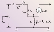
In Figure 3,

In Figure 4, when adding a source inductance Ls in the FET’s source lead, the input voltage can be rewritten as

Since


Then Vg can be expressed as


Thus, the equivalent input impedance is

is an “added” input impedance introduced by the source inductor, and the added resistive and reactive component both help to pull the S*11 closer to ?opt.

Normally, Ls should be a small inductor optimized according to Equation 5. Based on the analysis above, a small microstrip line (width = length = 16 mil) together with a via-hole was introduced on both of the source leads to work as a small inductor. According to the measured results, the microstrip lines actually pull the S*11 closer to ?opt while not changing the value for ?opt (necessary for NFmin). Since the feedback is negative, there is an accompanying decrease in gain with increasing feedback. In this circuit, the gain did not decrease too much.
Input Matching Network Design
Since the LNA operates around 3.5 GHz, a high pass filter is required for input matching. When pulling S*11 closer to ?opt = 0.32< –170°, the matching network should also maintain the gain.
In Figure 5, the input conjugate S11 is 0.38 < –162° after proper allocation of the capacitor, inductor and microstrip lines. Figure 6 is the equivalent circuit. According to the measured results, this input matching network will lead to S11 = –20 dB and NF = 0.82 dB. The measurement results are in line with the theoretical analysis and ADS simulation.
Passive DC biasing
Once the RF input matching has been established, the next step is to establish the DC biasing. Since the DC biasing conditions are Vgs = 0.59 V, Vds = 3 V and Ids = 60 mA, it is easy to determine the DC biasing


where
Vdc = power supply voltage, 3.6 V
Vds = device drain to source voltage, 3 V
Vgs = device gate to source voltage, 0.59 V
Ids = device drain to source current, 60 mA
Determining Device Values
To achieve low input return loss, low noise figure and high gain, the values for C1, TL43, L1 and TL24 in the simulation are established according to the analysis of the input matching network design. The width and length of L2 and L3 are determined according to the ADS simulation. The SRF (series resonant frequency) for C5 is selected to be 3.5 GHz to terminate the frequency around 3.5 GHz and thus help improve linearity. C3 and C6 are used as a low frequency bypass to terminate the high frequency second-order harmonics and thus help improve linearity. The resistor R5 helps terminate the low frequencies, and can improve the in-band stability by preventing resonant frequencies between the two bypass capacitors. Table 1 summarizes the bill of material for the LNA board.

Measured Performances of the ATF-54143 LNA at 3.5 GHz
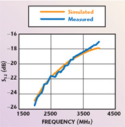
With a drain current of 60 mA, the measured and simulated performances of the LNA are compared with good agreement. Figure 7 shows a gain of 12.8 dB at 3.5 GHz and a noise figure of 0.82 dB is achieved (see Figure 8). Figure 9 shows the comparison between the simulated and measured input return loss, both of which are 20 dB at 3.5 GHz. The simulated and measured output return loss are shown in Figure 10, both of which are greater than 11 dB. The response is wide enough to cover the operating frequency range from 3.3 to 3.8 GHz. Figure 11 depicts the comparison for the isolation (S12), while Figure 12 is the comparison for OIP3.
Conclusion

Based on theoretical analysis and ADS simulation, this article demonstrates a 3.3 to 3.8 GHz WiMAX LNA built on a FR4 board material. Since it has a high linearity (P1dB> +19 dBm, OIP3 > +36 dBm), this LNA can also be used as a PA driver for radio cards and CPE. The measured RF results verify the feasibility of 3.5 GHz WiMAX designs built on a FR4 board. Over the 3.3 to 3.8 GHz operating frequency range, the FR4 board does not significantly impact the noise figure and gain.
Acknowledgments
The author would like to thank Eric Chan, Lim Chin-Liang and Abdullah Asrul-Sani of Agilent Technologies, Malaysia, for their valuable help and comments during the circuit tuning and validation.
References
1. I. Bahl, Lumped Elements for RF and Microwave Circuits, Artech House Inc., Norwood, MA, 2003, Chapter 13.
2. Data Sheet, “RO4000® Series High Frequency Circuit Materials,” Rogers Corp., 2002.
3. Data Sheet, “Agilent ATF-54143 Low Noise Enhancement-mode Pseudomorphic HEMT in a Surface-mount Plastic Package,” Agilent Technologies Inc., 2003.

4. I. Bahl and P. Bhartia, Microwave Solid State Circuit Design, John Wiley & Sons Inc., Hoboken, NJ, 1988, Chapter 7.
5. J. Engberg and T. Larsen, Noise Theory of Linear and Nonlinear Circuits, John Wiley & Sons Inc., Hoboken, NJ, 1995, Chapter 6.
6. S.A. Maas, Nonlinear Microwave and RF Circuits, Artech House Inc., Norwood, MA, 2003, Chapter 8.
