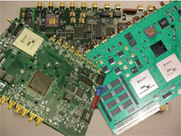
A dual-channel, very high speed data acquisition and real-time digital signal processing module has been developed that is useful in applications such as electronic warfare (EW), radar and software-defined radios. The board incorporates two Atmel AT84AS008VGL, 2.2 Gsa/sec, 10-bit analog-to-digital converters and up to three Virtex-4 field programmable gate arrays (FPGA). The board also has two high speed serial (Hotlink) interfaces and a VME64 interface.
Product Description
The board incorporates two Atmel AT84AS008VGL A/Ds that feature a maximum sample rate of 2.2 Gsa/sec at 10-bits with a 3.3 GHz full power input bandwidth. Their spurious free dynamic range (SFDR) is 58 dBc (7.4 effective bits at FS = 1.4 Gsa/sec, fIN = 700 MHz). A companion device, the AT84CS001, demultiplexes the high speed, 10-bit LVDS A/D outputs onto a 40-bit, differential bus running at ¼ of the sample rate. The A/D’s sampling delay and gain can be adjusted to support synchronizing and interleaving multiple A/D boards. The output of the demultiplexer is connected to a Virtex-4 using a 40-bit, differential bus and clock.
Also, on the new receiver board are sites for three Virtex-4 FPGAs. There is an XC4VSX55s directly connected to each A/D channel and also an XC4VLX200. High speed differential buses connect all three devices. The XC4VLX200 is used to implement the Hotlink and VME interfaces. A soft processor (CPU) is integrated into the XC4VLX200 for board level control and communication.
The CPU module is used to provide a user interface, local control, and to read and write from Flash. This module also provides an RS232 interface for test; a simple command set is used to configure the board and control data collection and processing. There are 64 Mbytes of flash memory that can be used to store FPGA configuration data.

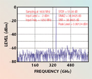
The high speed serial links are implemented using the CYP15G0101DXA HOTLink II™ transceiver from Cypress Semiconductor. It contains all of the logic to support the serialize/de-serialize (SERDES) function and clock recovery, and supports data rates from 200 to 1500 Mbaud. Figure 1 displays a downconverted 1250 MHz signal, sampled at 1600 Gsa/sec showing the receiver’s SFDR performance exceeding 55 dBc.
The VMEbus interface is designed to conform to the VME64x specification and requires the 160 pin connectors with the added ground pins and +3.3 V power pins. The interface was designed to support A32/D32 slave data transfer.
Typical power consumption is 60 W; all power is derived from the VME standard power supplies using on-board DC-DC converters. The board can be used in convection or conduction cooled applications and is rated for operation from –40° to +85°C.
Additional Capabilities
In addition, LNX can develop custom algorithms based on customer specifications as a result of the company’s significant investment in system simulation, algorithm development and FPGA logic synthesis tools. These tools allow the company to develop and simulate fixed-point DSP algorithms in Matlab™ and automatically convert those algorithms into VHDL for synthesis and implementation on the FPGAs. This allows LNX engineers to rapidly develop, simulate and test new algorithms without having to manually convert new algorithms to VHDL or Verilog.
Conclusion
A very high speed data acquisition and real-time DSP processing platform has been introduced that is ideal for use with EW, radar and software-defined radio applications. With the company’s in-house tools and capabilities, new receiver designs can be easily tailored, using lower cost design techniques as necessary to implement new requirements.
LNX Corp.,
Salem, NH
(603) 898-6800,
www.lnxcorp.com.
