Due to the fast development of wireless communications, a low cost, high performance, high integration technology is needed for system-on-a-chip (SoC) implementation. CMOS technology provides a good solution for SOC integration.1 Recent improvements of the standard CMOS process make it possible to implement RF blocks, such as low noise amplifiers, mixers, voltage-controlled oscillators (VCO), power amplifiers and T/R switches2 for operation at frequencies up to the 2.4 and 5 GHz bands. Also, a 2.4 GHz CMOS power amplifier with an output power of 20 dBm has recently been reported.3 The trend toward the goal of a single-chip transceiver radio or a radio-on-a-chip (RoC) with a medium-range transmitting power becomes more feasible.

Fig. 1 Architecture of a 2.4 GHz single-mixer transceiver.
In this article, a 2.4 GHz CMOS transceiver RF front-end is presented, which uses a single-mixer transceiver architecture4 (see Figure 1) for Bluetooth or wireless LAN (WLAN) applications. As shown in Figure 2, the transceiver RF front-end has a transmitter and a receiver RFIC. The transmitter includes a power amplifier with a diode linearizer and two T/R switches. The receiver RFIC contains a gain-controlled LNA and a passive switching mixer. The RF is from 2.400 to 2.483 GHz and the IF is at 280 MHz. The RFICs are fabricated with the 0.25 mm 1P5M standard CMOS process. The measurements are performed using an FR-4 PCB test fixture for each CMOS RFIC. All the RFIC PCB test fixtures are then connected into a single-mixer RF transceiver for extensive measurements of transmit and receive modes, including digital modulation test.

Fig. 2 Block diagram of the CMOS transmitter and receiver RFIC's developed for a single-mixer RF transceiver.

Fig. 3 Schematic of a 2.4 GHz, two-stage, cascode CMOS LNA with gain control

Fig. 4 Gain (a), noise figure (b) and allowed maximum power (c) for IMD3 <-40 dBC vs. control voltage.

Receiver Circuit Design
Gain-controlled LNA
The most important procedure in CMOS LNA design is to choose the right NMOS transistor channel width that has the lowest noise figure.5 A two-stage, 2.4 GHz CMOS LNA with a gain control circuit is shown in Figure 3. The cascode configuration is used to obtain better frequency response and stability. From experience, the transistor channel width of M2 is chosen to be 1/2 of that of M1 to assure stability. The Ls, Lg and Cgs of M1 form a 50 ? input impedance. Ls and Lg can be made by bond-wires. C1 provides an AC ground to the common gate stage and C2 isolates the power supply noise. C3 provides an AC ground to assure the parallel resonance will not be affected by other parasitic like bond-wires, test board microstrip line effects and supply noises. The gain control circuit is added by using a parallel variable resistance realized by using an NMOS transistor biased at Vds = 0 V.6

Fig. 5 Schematic of a 2.4 GHz CMOS passive switching mixer.

Fig. 6 Layout of the FR-4 PCB test fixture for the passive switching mixer measurements.
The simulated and measured LNA characteristics are shown in Figure 4. The measured input and output return losses are 25 and 19.4 dB, respectively, and the gain is approximately 15.8 dB. The measured input intercept point (IIP3) is –7.5 dBm. The gain tuning range and the noise figure versus the control voltage (0.2 ~ 2.5 V) are approximately 15.8 to 2.2 dB and 3.2 to 8.7 dB, respectively. The allowed maximum input power (for which IMD3 is set to be less than –40 dBc to test the linearity of the LNA) is also shown. It is observed that the allowed maximum input power is between –28 and 5.8 dBm for the control voltage set between 0.2 and 2.5 V. A summary of the simulated and measured results is shown in Table 1.

Fig. 7 Schematic of an L-C current combiner.
Passive Switching-mixer Circuit Design
A series-type 2.4 GHz CMOS passive switching mixer7 is shown in Figure 5. The most important procedure in a CMOS passive switching-mixer design is to choose the right NMOS transistor channel width, which has the lowest insertion loss and moderate port-to-port isolation. The switching pairs are 80 ?m NMOS transistors. To deal with the measurements of the three differential-ports (of the RF, LO and IF ports), the RF and LO test signal are split with 180° hybrid ring couplers, which can be seen in the layout of the FR-4 PCB test fixture of the mixer shown in Figure 6. The IF test signal is combined by a L-C current combiner (see Figure 7).

Fig. 8 Conversion gain vs. (a) LO power (Vgs = 0.65 V), (b) gate voltage (LO=5 dBm) and (c) input RF power.
The simulated and measured mixer characteristics are shown in Figure 8 and listed in Table 2. The measured input return losses of the RF and IF ports are 20 and 9.2 dB, respectively. As shown, the conversion loss is from 6.8 to 7.9 dB for a LO power from 0 to 10 dBm when the gate voltage Vgs is kept at 0.65 V. It can also be seen that the smallest conversion loss is 7.2 dB at Vgs = 0.65 V (LO = 5 dBm). The measured input P1dB is 4.5 dBm. Figure 9 shows that the measured noise figure is 11.8 dB. The measured input intercept point (IIP3) is 10.6 dBm.
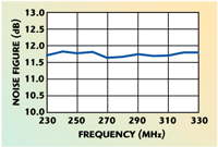
Fig. 9 Measured noise figure vs. frequency.
Receiver Performance Measurement
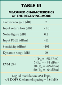
The chip micrographs of the LNA and the mixer in a CMOS receiver RFIC are shown in Figure 10. Figure 11 illustrates the receive-mode test for the RF transceiver. Figure 12 shows the measured performance of the receiving mode. Since an IF amplifier is not included due to the losses of the passive mixer (approximately 7 dB) and T/R switch (approximately 2 dB), the measured conversion gain is approximately 2 dB. The noise figure is 6.2 dB. The input 1 dB compression point is approximately –11 dBm. The input return loss (at the antenna-port of the T/R switch) is about –13 to –19 dB at 2.400 to 2.483 GHz.

Fig. 10 Micrograph of a 2.4 GHz, 0.25 ?m CMOS RF receiver RFIC showing the LNA and mixer.

Fig. 11 Receiver mode test for the single-mixer RF transceiver.

For the digital modulation test, a 384 kbps, ?/4 –DQPSK digital modulation signal with channel spacing of 384 kHz is applied to the RF transceiver. Figure 13 shows the measurement setup for the digital modulation test, which includes a vector signal generator and vector signal analyzer. The EVM (error vector magnitude) measurement results at different input power levels are shown in Figure 14; the measured EVM value is approximately 20 percent (for an input power of –94 dBm) and 1 percent (for an input power of –65 dBm) at 2.45 GHz. The receiving sensitivity is determined using
![]()
The SNR corresponding to an EVM of 20 percent is 14 dB, since

where
Es = energy of a symbol
Rs = symbol rate (= half of data rate)
N0 = noise power density
B = bandwidth
For a 4/p – DPSQ signal and a SNR of 14 dB, it can be determined that
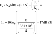 Hence, from the definition of the sensitivity
Sensitivity Si (dBm) =
–174+NF+Es/N0+10log (symbol rate)
= –174+NF+Es/N0+10log (192 ksps)
= –174+6.2+17+(10log192+30) = –98
where NF is the receiver noise figure, which is 6.2 dB. This value is consistent with the Es/N0 of 17 dB, obtained from the measured EVM of 20 percent at –94 dBm input power level. The difference of 4 dBm (98 – 94) may be due to the measurement deviation.

Fig. 12 Measured performance of the 2.4 GHz RF transceiver in the receive mode for conversion gain (a) and output power (b) vs. input power, and antenna port return loss (c) vs. frequency.

Fig. 13 Measured setup for the digital modulation test in the receive mode.
Since the typical accepted bit error rate (BER) for a communication receiver is 10–5, which corresponds to a required Es/N0 of 10 dB, the receiving sensitivity (at BER = 10–5) can be derived as –101 dBm (–94 + (10 – 17)). From the derived sensitivity and the measured input 1 dB compression point (–11 dBm), the receiver dynamic range (DR) can then be determined.
Dynamic Range = P1dB(input) –
Sensitivity = –11–101 = 90 dBm (5)
Table 3 summarizes the measured receiving mode characteristics of the 2.4 GHz CMOS RF transceiver.
Transmitter Circuit Design
Power Amplifier (PA) with a Diode Linearizer

Fig. 14 EVM measurements at Pin = -94 dBm (a) and -65 dBm (b).
In a CMOS PA design, the most important procedure is to choose the right NMOS transistor channel width that has the capability to generate enough power to the output load. Due to the low breakdown voltage and high knee voltage, the output power and efficiency of a CMOS PA is limited. It is experimentally shown that the P1dB of a gain-matched amplifier is 1 to 2 dB lower than when it is power-matched.6 This rule is used to predict the output stage transistor channel width, which is then precisely adjusted. The driver stage transistor channel width is usually set to be 1/3 of the output stage to insure that it can drive the output stage. Inductors and bypass capacitors play the same role of those mentioned in the CMOS LNA design procedure. L1 and Cgs of M2 form a parallel resonance to perform simply the interstage matching. The input of the PA is gain matched and its output is power-matched by using a software load-pull simulation. A resistor (approximately 1 k?), connected between gate and drain, can help to increase stability.
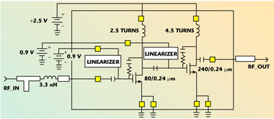
Fig. 15 Schematic of a two-stage, 2.4 GHz CMOS PA with a diode linearizer.
A two-stage, 2.4 GHz class-AB CMOS PA is shown in Figure 15. The design goal is to have an output power of more than 10 dBm. The output stage transistor gate is 240 ?m wide. The driver stage is chosen to be 1/3 the output transistor’s size. A diode linearizer is formed by an 80 ?m wide diode connected to the NMOS transistor.39 The circuit measurement is performed in an FR-4 PCB test fixture. As listed in Table 4, the measured input and output return loss is 10.4 and 12.7 dB, respectively. The linear gain is 13.2 dB and the power-added efficiency (PAE) is approximately 20 percent. Figure 16 shows a comparison of the measured power gain and PAE versus input power of a 2.4 GHz CMOS PA with and without a diode linearizer. It can be observed that the output P1dB increases from 10.2 to 13.6 dBm (approximately a 3.5 dB increase) and the PAE (at the 1 dB compression point) increases from 15.6 to 20.2 percent, respectively, when using the diode linearizer. The measured ACPR (under ?/4–DQPSK signal with a data rate of 48.6 kbps, a channel spacing of 30 kHz and a channel bandwidth of 24.3 kHz) is shown in Figure 17, which also shows the increase in linearity. As the data indicates, the ACPR increases from –30.3 to –38.7 dBc (when the main channel output power is set at 10 dBm). This shows that the diode linearizer can offer good improvement on the linearity of the PA when dealing with a signal with high variation of the envelope (like ?/4–DQPSK).
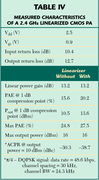
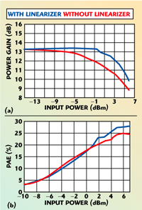
Fig. 16 Comparison of the measured power gain (a) and PAE (b) vs. input power with and without a diode linearizer.

Fig. 17 Measured ACPR of the PA (a) without the linearizer and (b) with the linearizer.
T/R Switch
The most important procedure in CMOS T/R switch design is to choose the right NMOS transistor channel width, which has the lowest insertion loss and highest isolation.89 By simply using an RF model simulation, measured results still show acceptable performance. As shown in Figure 18, there are some rules according to the relationship of resistance, capacitance and parasitic effects with insertion loss and isolation in a transistor for a CMOS series T/R switch design:
• When the series-arm is opened and the transistor gate-width becomes larger, the resistance Ron becomes smaller, the substrate parasitics become larger, and, due to these two factors, the insertion loss decreases first (Ron dominates) and then increases (substrate parasitics dominate).
• As the series-arm is closed and the transistor gate-width becomes larger, the capacitance Coff becomes larger, the substrate parasitics become larger, and, due to these two factors above, the isolation only decreases.

Fig. 18 Simple equivalent model of a transister in (a) opened and (b) closed conditions.
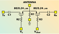
Fig. 19 Schematic of a series-type 2.4 GHz CMOS T/R switch.
By using the above two rules, the most suitable transistor gate-width is chosen according to the simulation results with an RF model and a 50 W match is assuraed for each port. A series-type 2.4 GHz CMOS T/R switch is shown in Figure 19. An 80/0.24 mm NMOS transistor is chosen for the series-arm. The control voltage is 2.5 V. Note that a resistance R1 is needed to assure a DC to ground biasing path. As listed in the data, the measured return loss of the Tx and Rx terminal is approximately 18 dB and that of the antenna-port is 22.4 dB. The isolation is approximately 17.7 dB. Figure 20 shows the insertion loss versus the input power. It can be seen that the insertion loss is about 2 dB and the input P1dB is approximately 18.6 dBm. A summary of the measured characteristics is shown in Table 5.

Fig. 20 Insertion losss vs. input power.
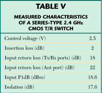
Fig. 21 Measured ACPR of the PA (a) without the linearizer and (b) with the linearizer.

Fig. 21 Chip micrograph of a 2.4 GHz, 0.25 ?m CMOS RF transmitter.

Fig. 22 Transmit mode test for the single-mixer RF transmitter.
Transmitter Performance Measurement
Figure 21 is a chip micrograph of the PA and the T/R switch in a CMOS transmitter RFIC. Figure 22 illustrates the transmit-mode test for the RF transceiver. Due to the loss of the mixer and T/R switch, two PAs are connected to achieve a higher gain. When in the transmit-mode test, the power of the LNA is turned off, and that of the PA is off when in receive-mode test.
Figure 23 shows the measured output power and gain compression as a function of the input power at 2.45 GHz. The gain is approximately 7.8 dB and the output P1dB is about 11.5 dBm. Note that, after subtracting the loss of the T/R switch (2 dB), the output P1dB of the transceiver is very close to that of the PA (13.6 dBm). It also shows that the output return loss (at the antenna-port of the T/R switch) is about –13 to –19 dB at 2.400 to 2.483 GHz.

Fig. 23 Measured performance of the RF transceiver in the transmit mode; (a) conversion gain and (b) output power vs. input power, and (c) output return loss at the antenna port of the T/R switch.

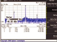
Fig. 24 The LO leakage power level in the transmit mode.
For the digital modulation test (384 kbps ?/4– DQPSK signal with channel spacing 384 kHz), as listed in Table 6, the EVM and ACPR values are approximately 1.8 percent and –45 dBc (at 5 dBm output power) and –4 percent and –32 dBc (at 10 dBm output power), respectively. Also, it is desired to know the LO leakage power level at the RF frequency (2.45 GHz) ± IF (280 MHz). Measured results in Figure 24 show that the measured LO leakage is approximately 35 and 50 dBc at 2.17 GHz (RF–IF) and 2.73 GHz (RF+IF), respectively. Table 6 summarizes the measured characteristics in the transmit mode of the 2.4 GHz CMOS RF transceiver.
Conclusion
The design and extensive measurements of 2.4 GHz, 0.25 mm CMOS RFICs for an RF transceiver have been presented. The RFICs are fabricated using the 0.25 ?m 1P5M standard CMOS process. With the RF at 2.400 to 2.483 GHz and the IF at 280 MHz, the CMOS RF transceiver uses a single-mixer architecture. The transmitter RFIC has a power amplifier with a diode linearizer and two T/R switches. The receiver RFIC consists of a gain-controlled low noise amplifer and a passive switching mixer. The measurements are performed using an FR-4 PCB test fixture for each CMOS RFIC. All RFIC PCB test-fixtures are connected to perform extensive measurements in the transmit and receive modes, including digital modulation tests.
A class-AB PA (13.2 dB gain and 13.6 dBm P1dB), a passive switching mixer (7.2 dB conversion loss), a gain-controlled low noise amplifier (15.8 to 2.2 dB gain and 3.2–8.7 dB noise figure) and a T/R switch (2 dB insertion loss and 17.6 dB isolation) are designed and combined with an RF bandpass filter (1.2 dB insertion loss) to form a single-mixer RF transceiver. In the transmit mode (two PAs are connected to achieve a gain of 7.8 dB), the output P1dB reaches 11.5 dBm after the loss of the T/R switch. For the digital modulation tests (384 kbps ?/4–DQPSK signal with a channel spacing of 384 kHz), the measured EVM /ACPR are approximately 1.8 percent/–45 dBc (Pout = 5 dBm) and –4 percent/–32 dBc (Pout=10 dBm), respectively. In the receive mode, a 2 dB conversion gain (without an IF amplifier), 6.2 dB noise figure and –11 dBm input P1dB are measured. For digital modulation measurements (384 kbps ?/4–DQPSK signal with channel spacing of 384 kHz), the EVM is 1 percent (Pin = –65 dBm) and 20 percent (Pin = –9 4 dBm), respectively. The receiving sensitivity is approximately –101 dBm (at BER = 10–5) and the dynamic range (DR) is 90 dB. The CMOS RF transceiver performance demonstrates that the standard 0.25 mm CMOS process has great potential for 2.4 GHz wireless transceiving communications.
Acknowledgments
The authors would like to thank the Chip Implementation Center (CIC) of the National Science Council, Taiwan, ROC, for its support of the TSMC CMOS process. This work was supported by the National Science Council, Taiwan, ROC, under Grant NSC 93-2215-E-006-022.
References
1. T.H. Lee, The Design of CMOS Radio-frequency Integrated Circuits, Cambridge University Press, New York, NY, 1998.
2. K. Yamamoto, et al., “A 2.4 GHz Band, 1.8 V Operation Single-chip Si-CMOS T/R-MMIC Front-end with a Low Insertion Loss Switch,” IEEE Journal of Solid-State Circuits, Vol. 36, No. 8, August 2001,
pp. 1186–1197.
3. C.C. Yen and H.R. Chuang, “A 0.25 mm 20 dBm 2.4 GHz CMOS Power Amplifier with an Integrated Diode Linearizer,” IEEE Microwave & Wireless Component Letters, Vol. 13, No. 2, February 2003,
pp. 45–47.
4. S.Y. Liu and H.R. Chuang, “2.4 GHz Transceiver RF Front-end for ISM-band Digital Wireless Communications,” Applied Microwave and Wireless, June 1998, pp. 32–48.
5. D.K. Shaeffer and T.H. Lee, “A 1.5 V 1.5 GHz CMOS Low Noise Amplifier,” IEEE Journal of Solid-State Circuits, Vol. 32, No. 5, May 1997, pp. 745–759.
6. “GaAs AGC Amplifier for CDMA Cellular Phone Systems,” OKI Technical Review, Vol. 63, No. 158, April 1997.
7. A.R. Shahani, D.K. Shaeffer and T.H. Lee, “A 12 mW Wide Dynamic Range CMOS Front-end for a Portable GPS Receiver,” IEEE Journal of Solid-State Circuits, Vol. 32, No. 12, December 1997, pp. 2061–2070.
8. S.C. Cripps, RF Power Amplifier for Wireless Communications, Artech House Inc., Norwood, MA, 1999.
9. T. Yoshimasu, M. Akagi, N. Tanba and S. Hara, “An HBT MMIC Power Amplifier with an Integrated Diode Linearizer for Low Voltage Portable Phone Applications,” IEEE Journal of Solid-State Circuits, Vol. 33, No. 9, September 1998.
10. F.J. Huang, et al., “A 0.5 mm CMOS T/R Switch for 900 MHz Wireless Applications,” IEEE Journal of Solid-State Circuits, Vol. 36, No. 3, March 2001,
pp. 486–492.
11. A. Zolfaghari and B. Razavi , “A Low Power 2.4 GHz Transmitter/Receiver CMOS IC,” IEEE Journal of Solid-State Circuits, Vol. 38, No. 2, February 2003,
pp. 176–183.
