Because of the unique characteristics of the specification, LTE mobile infrastructure will require components with high linearity and low loss in very small form factors; they must also operate with low power consumption. Manufactured using UltraCMOS, the Peregrine PE43204 digital step attenuator (DSA) meets these complex demands. It is best suited for use in the signal chain to adjust power levels and is specifically designed for LTE infrastructure applications such as base stations and remote radio heads.
Typically used in the receive path for gain control, the PE43204 DSA features a fast switching speed, which allows attenuation to be added quickly to protect the receiver and prevent over-driving the analog-to-digital converter. The new DSA takes advantage of the company’s proprietary HaRP™ technology that dramatically improves linearity and eliminates gate lag or phase drift, which results in a very fast settling time.

Figure 1 PE43204 attenuation error vs. frequency (25°C).
Specifically, the PE43204 features a typical switching time of 26 ns with a typical attenuation accuracy of +0.2 dB across a wide operating range of 50 MHz to 3 GHz (see Figure 1). In comparison, many GaAs DSAs demonstrate a typical switching speed of 130 nS, which is more than 4x slower than the UltraCMOS DSA.
In some receiver architectures fast switching speed is imperative to protect the receive path from damage when strong blocking signals are present, and it is also key for gain control on the base station. As throw counts increase for LTE, this specification becomes even more important. Faster switching speeds and shorter settling times lead to more reliable and more accurate performance, and UltraCMOS inherently offers these advantages.
If multiple-input and multiple output, or MIMO, antenna technology is implemented this increase in functionality and signal paths increases the need for smaller form factors (and higher integration in order to control component count). For instance, in a 2 × 2 configuration there will be a DSA in each transmit and receive path. The cost of deploying new LTE services will also keep pressure on minimizing the bill of materials and design complexity. Clearly, the need for higher integration as well as smaller sizes and higher performance is critical.

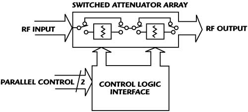
Figure 2 Functional block diagram for PE43204 DSA including on chip integrated control logic.
Recognizing this need, designers at Peregrine took advantage of the ability to realize logic in CMOS and integrated a parallel control interface programming logic in the PE43204, all while housing it in an ultra-compact 12-lead 3 × 3 × 0.85 mm QFN package (see Figure 2).

Figure 3 PE43204 input IP3 vs. attenuation setting (25°C).

Figure 4 PE43204 insertion loss vs. temperature.
The challenges of LTE design do not stop with switching speed and board real estate. Specifically, on the downlink, LTE implementation of orthogonal frequency division multiplexing (OFDM) uses several closely spaced orthogonal subcarriers make up a resource block (RB). The number of RBs will vary depending upon the system’s bandwidth, but generally, 1RB is equivalent to twelve 15 kHz subcarriers. The use of RBs complicates receiver design, especially in terms of adjacent channel selectivity because the LTE specification notes that a very large in-band interferer is located only 1RB away. To be successful, devices with high linearity and isolation will be required to meet this challenge.
While maintaining a best-in-class typical input third order intercept point (IIP3) of +61 dBm, the PE43204 DSA demonstrates typical insertion loss of 0.6 dB and electrostatic discharge (ESD) of 2 kV (see Figures 3 and 4). High data rate systems, like LTE, benefit from higher linearity and low loss like the specifications demonstrated by the PE43204 DSA. In addition, components with high ESD ratings are highly desired in the manufacturing process to reduce the likelihood of ESD damage during assembly.
Despite their need for higher performance and more circuitry packed into an IC, designers of LTE systems also need to limit or reduce overall system power consumption, and many want to move towards ‘greener’ semiconductor processing choices. RF CMOS technology’s advantages of low power are well known. UltraCMOS technology is a CMOS process where a 50 to 100 nm silicon film is formed directly on a sapphire substrate. This provides for fully-depleted devices with little or no body charge under the gate. As a result, UltraCMOS processing delivers faster devices with reduced power consumption (as compared to GaAs) as well as excellent linearity and high isolation. Also, UltraCMOS does not use Arsenic. The PE43204 DSA, for instance, is biased from a 3 V supply with power supply current of 8 µA typical. These advantages make UltraCMOS devices in general (and the PE43204 DSA in particular) an excellent match for the rigorous demands of next-generation communications systems and LTE.
Peregrine Semiconductor
San Diego, CA
(858) 731-9400
www.psemi.com
