
This article presents the performance of a Ka-band bandpass filter (BPF) using a coplanar waveguide (CPW) topology on an Al2O3 substrate. A copper (Cu) metallization was also used in this investigation to improve the characteristics of the filter. The measured results of the BPF, with a chip size of 2423 × 424 µm, show a return loss of 25.3 dB and an insertion loss of 0.6 dB at 27 GHz. A comparison between the simulated and experimental results shows good agreement. The overall filter characterization exhibits a broad bandwidth of 18.8 to 38.2 GHz, a high return loss and a low insertion loss, which illustrate that the BPF shows favorable RF characteristics in Ka-band with a compact circuit size.
The communication applications have increased noticeably in recent years. Apparently, the RF channel bandwidth allocated to communication system applications is approaching saturation. The providers of communication systems are now interested in the microwave band for the next-generation terrestrial systems, including military and satellite communication systems in Ka-band. Several researchers1,2 have reported that microwave monolithic integrated circuits (MMIC) using coplanar waveguide have been adopted in transmitter communication systems. In the CPW structure, the ground plane is placed on the top surface of the substrate. Thus, many advantages have been obtained with this CPW schematic layout, such as unnecessary back-side fabrication, good electronic isolation property and compact drawing in the circuit layout.1-3
As clearly shown in some review papers, CPW has been extensively studied for MMIC applications. However, little attention has been devoted to the conductor losses in the signal transmission path.2,3 A copper metal, with an extremely low electrical resistivity (1.7 × 10⁻⁸ Ωm), could significantly improve the insertion loss in the BPF.4 This study investigated a Ka-band BPF circuit using a CPW structure and a copper metallization on the Al2O3 substrate. A Ka-band BPF was fabricated and its S-parameters were measured with a vector network analyzer. The results demonstrated that the fabricated Ka-band BPF exhibited favorable MMIC characteristics within a small size.
Design and Fabrication of a Ka-band Bandpass Filter

Figure 1 Schematic of the CPW Ka-band bandpass filter.

Figure 2 Equivalent circuit of the Ka-band bandpass filter.
The Ka-band BPF circuit was designed using a CPW structure. Figure 1 shows the schematic layout of the Ka-band BPF, which uses two series open stubs with a characteristic impedance Z0 = 50 Ω and a length (l), which was designed to be approximately a quarter wavelength at the Ka-band center frequency (eff), that is, l = λeff/4.5 Ports 1 and 4 are the input and output of the filter, while Ports 2, 3, 5 and 6 are connected to ground. The lumped equivalent circuit model of the BPF is shown in Figure 2. In effect, each open stub is equivalent to three LC tanks (L1/C1, L2/C2 and L3/C3) with an air-gap (C0) series connection. This circuit permits a low transmission loss and easy fabrication.3 These resonators, with LC tanks, can operate in a wideband BPF. The resonators are operating in a mixed coupled mode, meaning partially magnetically and partially electrically coupled.

Figure 3 Microphotograph of the Ka-band bandpass filter fabricated on an Al2O3 substrate.
The S-parameters of the coupled resonating filter were simulated with the Advanced Design System (ADS), and the effect of the electric-magnetic coupling within the Ka-band BPF layout were computed with the HP-Momentum. Subsequently, the Ka-band BPF was laid-out and fabricated on an Al2O3 substrate 0.5 mm thick and with a conductor layer 2 µm thick, consisting of a Ti layer, 300 Å thick, to enhance adherence, the copper layer and a thin Au layer, 2000 Å thick, to prevent oxidation. Figure 3 shows a microphotograph of the Ka-band BPF, with a chip area of 2423 × 424 µm.
The S-parameters of a Ka-band Bandpass Filter

Figure 4 Measured and simulated S11 of the bandpass filter.
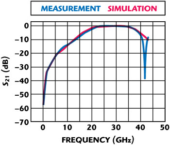
Figure 5 Measured and simulated S21 of the bandpass filter.
Figures 4 and 5 show the measured and simulated S-parameters of the Ka-band BPF. A simulated insertion loss (S21) of -0.6 dB and return loss (S11) of -10 dB were obtained within a bandwidth of 21.6 GHz, in the range 17.2 to 38.8 GHz. The BPF showed an input return loss exceeding -20 dB, from 25 to 35 GHz, in both measurements and simulation, as well as a maximum simulated return loss of -55 dB at 30 GHz.
The results indicate that the measured return loss is slightly degraded and shifted in frequency, compared with the simulation. The most likely explanation was that the variations in fabrication might be the cause of the negligible shift in the center frequency and the small degradation in the return loss. The simulated and measured S21 results agree fairly well, with the insertion loss remaining approximately constant in the range of 20 to 35 GHz. Overall, the S-parameters characterization confirms the low insertion loss and high return loss in this Ka-band BPF.

Finally, the S-parameters of the Ka-band BPF are summarized in Table 1. The experimental results appeared to be consistent with the simulation values. These S-parameter results indicate that the Ka-band BPF filter was well designed, demonstrating that the CPW structure with copper metallization on an Al2O3 substrate is adequate for the MMIC applications.
Conclusion
In this article, a Ka-band bandpass filter, using a CPW structure on an Al2O3 substrate with a copper metallization, was described. The use of copper metallization, which has a high conductivity, can reduce the insertion loss and improve the return loss of the circuit. The Ka-band BPF design uses two series open stubs with a characteristic impedance Z0 = 50 Ω, whose lumped element equivalent circuit consists of three LC tanks. The measured S-parameters agreed well with the simulation values. The Ka-band BPF exhibits a low insertion loss and a high return loss, which shows that a CPW structure with copper metallization on an Al2O3 substrate should be adopted for MMIC applications.
References
1. M. Muraguchi, T. Hirota, A. Minakawa, K. Ohwada and T. Sugeta, "Uniplanar MMICs and Their Applications," IEEE Transactions on Microwave Theory and Techniques, Vol. 36, No. 12, December 1988, pp. 1896-1901.
2. A.Q. Liu, A.B. Yu and Q.X. Zhang, "Broadband Bandpass and Bandstop Filters with Sharp Cut-off Frequencies Based on Series CPW Stubs," 2006 IEEE MTT-S International Microwave Symposium Digest, pp. 353-356.
3. M. Riaziat, I. Zubeck, S. Bandy and G. Zdasiuk, "Coplanar Waveguides Used in 2 to 18 GHz Distributed Amplifier," 1986 IEEE MTT-S International Microwave Symposium Digest, pp. 337-338.
4. C.S. Wu, H.C. Liu, Z.P. Liu and H.C. Chiu, "Compact K-band Bandpass Filter on High-k LiNbO3 Substrate," Solid State Electronics, Vol. 51, No. 6, June 2007, pp. 965-968.
5. J. Helszajn, Microwave Planar Passive Circuits and Filters, John Wiley & Sons Ltd., Chichester, UK, 1994.
Chia-Song Wu received his MSEE degree from Tsing Hua University, Hsinchu, in 1985, and his PhD EE degree from National Central University, Chungli, Taiwan, in 1998. In 1986, he joined the Chung Shan Institute of Science and Technology (CSIST), where his focus was on infrared detector technology. In 2003, he joined the EE department of Vanung University. His current research is on microwave and millimeter-wave integrated circuits.
Hsing-Chung Liu received his PhD EE degree from Kent State University in 1985. That same year he joined the Chung Shan Institute of Science and Technology (CSIST), where his focus was on infrared detector technology. In 2002, he joined the Dean of the R&D office at Vanung University. His current research is on microwave and millimeter-wave integrated circuits.
Hsien-Chin Chiu received his BS and PhD degrees in electrical engineering from National Central University, Chungli, Taiwan, in 1998 and 2003, respectively. He joined WIN Semiconductors Corp., Tao Yuan, Taiwan, where he was engaged in research and development of 6-inch GaAs PHEMTs and related integrated circuits. In 2004, he joined the EE department faculty team of Chang Gung University to focuses on microwave and millimeter-wave integrated circuits, fiber optic communication circuits and nano-technology.
Yi-Feng Lin received his MS degree in electronic engineering from Chang Gung University, Tao Yuan, ROC, in 2007. He is now a technology research engineer at Cyntec Corp., Hsinchu. His research interests include RFIC design and measurements and microwave passive devices.