 Over the last few years, the transition from analog to digital RF technology has signaled the need for high performance digital logic at higher data rates. The evolution of high speed digital communication demands more emphasis on S-parameter measurements, the ability to measure lower jitter, and more widespread use of differential circuits to provide noise immunity. These new requirements necessitate high speed logic and control circuits with lower random and deterministic jitter specifications, lower propagation delay, reduced data skew values and lower power consumption.
High speed logic is a key requirement in many wideband data acquisition and test systems, high capacity microwave or optical communications, and real time digital imaging. In these systems, the common design trend is to simplify the complexity of all of the stages from signal acquisition (the antenna) to analog-to-digital conversion (ADC), resulting in digitization of RF signals at higher sample rates. These higher data rates have caused more stringent specifications to be placed on the high speed interface and control logic devices.
To meet all of these requirements, Hittite Microwave began introducing a new line of 13 Gbps digital building blocks in early 2008. Most of these early products operated from -3.3 V supplies, provided adjustable output voltage swing capability, but with unique pinouts. Over time Hittite has significantly expanded the line, introducing a total of 23 SMT 13 Gbps logic devices in all. The product line features many -3.3 V devices with faster rise times, fixed or programmable output voltages, as well as versions with very competitive industry-compatible pinouts. Hittite’s strong commitment to the high speed logic product line continues, and now high performance versions operating from a single +3.3 V supply are available.
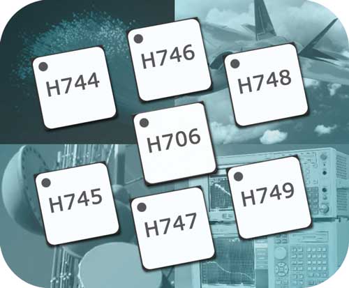
This new family of +3.3 V devices includes the HMC706LC3C NRZ-to-RZ Converter, the HMC744LC3C 1:2 Fanout Buffer, the HMC745LC3C XOR/XNOR gate, the HMC746LC3C AND/NAND/OR/NOR gate, the HMC747LC3 D-Type Flip Flop, the HMC748LC3C 2:1 Selector and the HMC749LC3C T-Flip Flop with reset capability (see Table 1). These logic devices may be used individually, or in combination to implement many critical digital subsystems spanning a myriad of applications, including broadband test equipment, ATE, military communications, radar, frequency synthesis, 10/100G Ethernet and SONET/SDH optical systems.

The HMC706LC3C is a NRZ-to-RZ Converter designed to support data transmission rates up to 13 Gbps and clock rates up to 13 GHz. During normal operation RZ data is transferred to the outputs on the positive edge of the clock, while negative edge-triggered applications are supported by reversing the clock inputs. Ideal for use in SONET OC-192 equipment, Mach-Zehnder optical modulators, 10 Gbps Ethernet applications and broadband test equipment, the HMC706LC3C provides typical rise and fall times of 15 and 13 ps, respectively. The device also exhibits 275 ps propagation delay and 2 ps of deterministic jitter while dissipating only 594 mW.
The HMC744LC3C 1:2 Fanout Buffer distributes precise clock or data signals in high performance applications. The device provides buffering capability for clock frequencies up to 13 GHz and serial data transmission rates up to 13 Gbps. The HMC744LC3C Fanout Buffer also provides very low data skew (< 2 ps) between data ports, which is ideal for critical time domain measurements since any skew between data ports may create race conditions. The HMC744LC3C is also ideal for bit-error-rate testing (BERT) applications since it helps designers to reduce the complexity of the clock distribution chain. The HMC744LC3C also exhibits fast rise and fall times of 22/20 ps and a propagation delay of 120 ps. The device exhibits less than 2 ps of deterministic jitter, less than 200 fs of random jitter and typically dissipates 287 mW.
The HMC745LC3C provides either an XOR or XNOR logic function. When configured as a XOR gate, the HMC745LC3C may be used to generate inverted data streams or may be used to implement a phase detector or a bit-error rate detector. The HMC745LC3C provides a typical propagation delay of 95 ps and typical rise and fall times of 21/19 ps while dissipating only 240 mW.
The HMC746LC3C may be configured to provide either AND, NAND, OR or NOR logic functions, providing system designers with maximum utility from a single device part number. When this device is configured as an AND gate, it may be used to gate high speed clock or data signals. The HMC746LC3C is ideal for this application since it provides high isolation of 50 dB in the off mode. The device also exhibits typical rise and fall times of 22/21 ps, and less than 2 ps of deterministic jitter while dissipating only 230 mW.
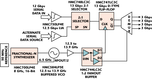
The HMC747LC3C D-Type Flip Flop is also designed to support data transmission rates up to 13 Gbps and clock rates up to 13 GHz. During normal operation, the data is transferred to the outputs on the positive edge of the clock, but for application flexibility, the clock inputs may be reversed to support negative edge-triggered applications. This device also exhibits a very low set up-and-hold time of less than 6 ps. The HMC747LC3C also provides excellent clock phase margin of 320 degrees at 13 GHz. This specification permits very robust system timing, and allows for a large range of clock data drift. Since the HMC747LC3C exhibits less than 2 ps of deterministic jitter and provides a propagation delay of 105 ps, this device may also be used in a wide range of applications where data bit streams need to be retimed as they travel across high speed system backplanes (see Figure 1). The rise and fall times are typically 22/20 ps and the device typically dissipates 264 mW.

Figure 1 Typical example where 12 Gbps serial data stream is retimed and demultiplexed.
The HMC748LC3C is a 2:1 Selector designed to support data transmission rates of up to 13 Gbps and selector port operation of up to 13 GHz. The selector routes one of the two single-ended inputs to the differential output upon assertion of the appropriate select port. The HMC748LC3C is ideal for redundant path switching or built-in test applications, since propagation delay is only 125 ps while rise and fall times are both 22 ps. The device exhibits only 2 ps of deterministic jitter while dissipating 250 mW.
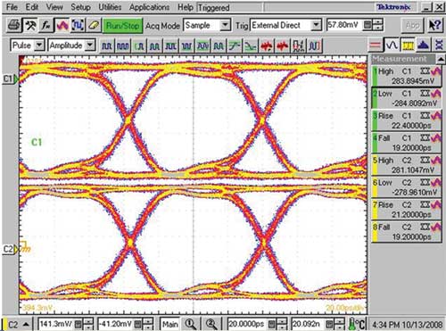
The HMC749LC3C is a T Flip Flop with reset capability supporting clock frequencies as high as 26 GHz. During normal operation, with the reset pin not asserted, the output toggles from its prior state on the positive edge of the clock. This results in a divide-by-two function of the clock input. Asserting the reset pin forces the Q output low regardless of the clock edge state (asynchronous reset assertion). Reversing the clock inputs allows for negative edge-triggered applications. Propagation delay is typically 95 ps while rise and fall times are 18 and 17 ps, respectively. Ideal as a high speed frequency divider, the HMC749LC3C exhibits only 2 ps of deterministic jitter while dissipating 270 mW. See Figure 2 for output eye diagram.

Figure 2 HMC747LC3C output eye diagram using Agilent N4901B serial BERT with 12 Gbps 215-1 PRBS data pattern.
Each of these high performance logic devices feature an output level control pin, VR, that permits signal loss compensation that can occur when very high speed signals travel over transmission lines. This feature is also ideal for signal level optimization. In this way, the signal output level could be reduced to generate lower output voltage swings, permitting faster rise time and lower propagation delay. The output signal level can be adjusted by either applying a voltage directly to VR, or by connecting the pin to ground with a suitable resistor value. In some applications this voltage may be accurately set with a low-cost DAC. The programmable differential output voltage swing may be set anywhere in the range from 0.6 to 1.2 V.
The current mode logic (CML) inputs and outputs of this family of logic devices provide a wide common mode operating range. These devices can accommodate input signals in the range of +2.1 to +3.8 V, and can operate with a DC supply in the range of +3.0 to +3.6 V. These devices also feature over-voltage protection on the power supply and ground pins, and all of the inputs and outputs are ESD protected.

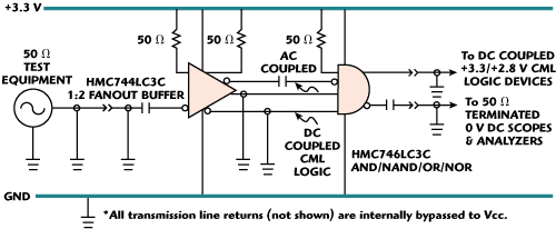
Figure 3 High speed logic showing various interfacing and termination schemes.
As shown in Figure 3, these 13 Gbps logic devices may be used to support a wide range of termination schemes accommodating both ac and dc coupling requirements. These devices feature differential inputs and outputs, which are DC coupled and terminated on chip with 50 Ohm resistors to ground. With the exception of the HMC748LC3C 2:1 Selector, the inputs or outputs of this family of devices may be used in either single-ended or differential modes. Unfortunately, many high speed logic devices available on the market today suffer severe degradation when used in single-ended modes. One of the key features of these Hittite logic devices is that excellent jitter performance is maintained even when they are operated with single-ended inputs and outputs.
It should also be noted that while inputs and outputs are terminated to the positive supply, all transmission line returns are at ground and are internally bypassed on-chip to support high speed operation. This allows the CML inputs and outputs to be connected to RF test equipment referenced to ground.
The HMC706LC3C, HMC744LC3C, HMC745LC3C, HMC746LC3C, HMC747LC3C, and the HMC749LC3C logic devices represent the first products in this new +3.3 V logic family; additional products with complementary functions will be released in the coming months. These devices are specified for operation from -40 to +85°C, and are housed in ceramic RoHS compliant 3 x 3 mm SMT packages.
In addition to the seven +3.3 V logic devices discussed here, Hittite offers a wide range of -3.3 V, 13 Gbps/13 GHz logic products to cover a variety of design specifi--cations. The HMC670LC3C through HMC673LC3C series were the first generation of 13 Gbps devices operating from -3.3 V supply, but with proprietary pinouts, adjustable voltage outputs and rise/fall times in the 24/22 ps range. The HMC678LC3C and HMC679LC3C also provide proprietary pinouts, adjustable voltage outputs but with faster rise/fall times in the 17/15 ps range. The HMC720LC3C through HMC723LC3C series also feature proprietary pinouts, and adjustable voltage outputs, but with faster rise times than the original HMC670LC3C through HMC673LC3C series. The HMC724LC3C through HMC729LC3C are pin-compatible industry replacements with rise/fall times as fast as 17/15 ps. To cover OC-768 market requirements, Hittite recently released four 43/50 Gbps connectorized logic devices that are housed in miniature hermetically sealed modules and operate from -3.3 V, while consuming less than 690 mW.
Designers looking for versions of these products with alternate pinouts, alternate DC power supply voltages or higher operating speeds should contact Hittite Microwave directly. Multiple logic functions may also be combined to provide products with higher levels of integration, and these may be made available in SMT packages or module format to meet the needs of custom applications.
Hittite Microwave Corp.,
Chelmsford, MA (978) 250-3343,
www.hittite.com.
RS No. 303
