 A new range of high power, broadband amplifiers has been developed to capitalize on the inherent advantages of Gallium Nitride (GaN). With instantaneous bandwidths of 2 to 6 GHz and high reliability, the AS0206 family of amplifiers is well suited to several markets. In particular, its inherent reflected-power tolerance makes it appropriate for the needs of the EMC test industry (RF immunity testing to 61000-4-3) and for the testing of high power RF components.
High reliability combined with compact size and light weight also make the family suitable for use in commercial applications where space is at a premium and portability can be used advantageously. The product incorporates a number of important key features including a comprehensive built-in test (BIT) capability and the potential for retrospective upgrading of the amplifier’s initial power capability.
The GaN Advantage
The inherent properties of GaN have a number of advantages to offer the amplifier designer. A major one is that the transistor structure enables the development of product that allows operation into high VSWR loads, including short and open circuits, without the need for protective circuits or isolators. The higher gains of GaN transistors, compared to those of competing technologies, reduce both the overall transistor count and the number of combining stages required. Operation from high voltages results in a less complex power supply design, an important feature in determining the overall reliability of an amplifier structure.
Compared to packaged GaAs MESFETs, GaN HEMTs have lower input and output capacitances that, when combined with a higher Ft, simplifies the design task of matching over multiple octave bands. This may in turn lead to a subsequent reduction in production tuning requirements when compared with similar GaAs FET-based multi-octave band amplifiers.

Fig. 1 Power density comparison of competing solid-state technologies.
GaN has a power density at P1dB, in W/mm, of around eight times that of GaAs. This power density can lead to significant size and weight reduction in applications that demand it. Figure 1 compares the power densities, at P1dB, of competing power technologies.

Fig. 2 AS0206 topology follows a Corporate Structure Architecture approach.
AS0206 Architecture
The amplifier topology adopts a Corporate Structure Architecture (CSA) approach, as shown in Figure 2. The name comes from the similarity of the layout of the microwave building blocks to that of a corporate organization chart, but turned 90° clockwise. The advantages of the CSA design methodology have been proven in the company’s existing microwave range and the new amplifier family derives identical benefits from that topology.
The building block of the amplifier’s output rank is a 2 to 6 GHz, 19 W P1dB power module, with a typical gain of 15 dB. Concentrating on the development of a single common power module has the virtue that a high percentage of engineering resources (microwave, electrical, thermal, mechanical) can be focused to design a component around which a reliable system can be built..
Output Rank Power Module
The transistor at the heart of this module is the CGH-40010, a Gallium Nitride HEMT from Cree Inc. A combination of simulation work using the supplied large-signal model, supplemented by data collected within MILMEGA, has brought about the development of high quality matching networks that require minimal tuning to be applied at the manufacturing stage. These matching circuits are optimized for P1dB performance and the transistor is used in a balanced pair configuration.

Fig. 3 P1dB performance of the 20 W module vs. frequency.
Power is developed within the module by combining two balanced pairs in parallel, using one level of quadrature combining. This, in addition to the inherent robustness of the GaN devices, enables the modules to absorb 100 percent reflected power, even when the module is operating at full output power. This can be a significant benefit to the system designer if the amplifier is required to operate into high VSWR conditions. The power performance of the module over the band of interest is shown in Figure 3.
Automated Biasing
Each module has the capability of performing an automated bias routine when commanded via an external ASCII communications terminal. The individual device current settings, which need to be imposed to optimise system performance, are input to the module. Each individual device is then interrogated and its pinch off voltage and quiescent operating point determined. With this information stored, the modules can then be biased optimally for the required mode of operation.
Output Combiner
In designing the final output combiner it was vital that the insertion loss from input to output was kept to an absolute minimum, thus reducing the gain and power requirements on the system pre-amplifier stages. The final design consists of a two-layer cascade of two input, resistorless Wilkinson style combiner structures. The resistors are not required as all inputs are matched in phase and amplitude.

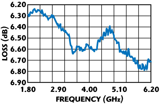
Fig. 4 Performance of the four-way combiner.
The completed combiner/coupler operates over the 2 to 6 GHz range and has an integrated coupler that provides forward and reverse outputs for sampling and measurement of incident/reflected power. Figure 4 shows the typical measured through path performance for this structure.
Bit and Control System
The overall control and sensing of the amplifier system is partitioned between three separate processors. The first processor, the central control processor, controls and monitors all system modules and provides the BIT functionality. Key parameters, including voltage and current consumption, are monitored for all modules. Modules in the output rank are monitored via direct connections to the central control processor. Less critical modules are monitored every few milliseconds via a multiplexer. A fault causes one of a column of LEDs to light. For convenience, the column is visible through the amplifier front panel.
A second processor, the local control processor, acts as the interface between the front panel control/indicator and the central control processor. It also senses and displays the forward and reflected RF power levels.
Finally, the communications processor acts as the interface between the central control processor and the outside world. Each processor has in-circuit programming capability, enabling the software to be updated.

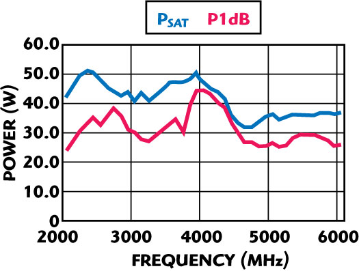
Fig. 5 Final system power performance.
The Final System
The amplifier features internal couplers for ease of measurement of reflected and incident power removing the need to utilize an external component with the associated power loss. The power achieved in the final system is shown in Figure 5 The AS0206 delivers a P1dB performance of 50 W minimum, with a Psat minimum of 75 W and a typical gain of 47 dB.
Conclusion
The inherent benefits of GaN power transistor technology have been combined with the CSA design approach, together with distributed embedded intelligence to create a robust power amplifier family providing high reliability, exceptional power density, ease of power upgrade and portability across the 2 to 6 GHz band.
MILMEGA,
Isle of Wight, UK
+44 (0) 1983 618004,
www.milmega.co.uk
RS No. 302
