RF-MEMS switches offer a number of advantages for switching in the gigahertz range because of their low insertion loss, high linearity and low power consumption.1 Several publications have reported on the performance of such switches, but more for non-packaged ‘naked’ samples. It is clear that the packaging process and the packaging environment can have a large impact, both negative and positive, on the functionality and reliability of these switches. A first possible impact of packaging on a switch is the packaging temperature profile. Often these temperature steps are higher than any step seen by the device before packaging and can, for certain switches, have detrimental effects.2,3 A second direct problem of packaging is out-gassing of the packaging material. Especially for ohmic switches, this can have a direct impact on the contact resistance.3 However, the package can also be used to control the pressure inside the cavity, in this way affecting the speed of the switch. The package can also protect the switch against the environment and, as such, solve several switch reliability problems in an indirect way. In this article, the two latter issues are discussed: the effect of pressure on the functionality of the switches and the influence of the environment (N2 versus air) on the reliability of the switches. The results given are for zero-level packaged capacitive RF-MEMS switches.
Switch and Zero-level Package
A schematic cross-section of a typical capacitive RF-MEMS switch is shown in Figure 1. The structure is essentially a coplanar waveguide (CPW) with an aluminum “bridge” above it and a dielectric layer located on top of the CPW. A number of etch holes are present in the bridge. When the bridge is up, an RF signal can propagate under the bridge to the other side. Application of an actuation voltage between the bridge and the CPW inner conductor causes an electrostatic attractive force between them, which pulls the bridge down. In the down-state, the capacitance formed by the metal/dielectric/bridge metal stack is large, causing a large mismatch; the RF signal is reflected and the switch is off. A MEMS package has to protect the device against external influences such as pressure, humidity, chemicals and particles. For MEMS processed on a wafer, it is mandatory to encapsulate them at the wafer level, in order to prevent exposure of the free structures to particles and debris produced during the dicing and handling process. For most switches, this process should be done at relatively low temperatures. Two sealing methods, typically used at IMEC, are metal/solder sealing or polymer (BCB) sealing, as shown in Figure 2.1,4,5 The metal sealing has the advantage to be hermetic, but it requires processing on the MEMS substrate. The BCB sealing requires only processing on the top cavity and at the same time provides electrical isolation but does not provide a hermetic seal. Figure 3 shows an example of RF-MEMS switches packaged on wafer level using a glass cap and BCB seal.6

Fig. 1 Schematic cross-section of a capacitive RF-MEMS device.

Fig. 2 Schematic picture of (a) metal/solder sealing and (b) polymer (BCB) sealing of MEMS switches.

Fig. 3 Example of zero-level packaged capacitive RF-MEMS switches using a glass cap and BCB sealing.
Influence of the Packaging Temperature
The bridge of the RF-MEMS switch is, in general, made of metal, such as Au-, Pt- or Al-alloy. During packaging, the switch will be subjected to different temperature steps. The BCB process, for example, typically requires a curing step at about 250°C.7 A question that arises is whether the metal of the MEMS bridge can stand this temperature. This was investigated by Modlinski, et al. for several Al-alloys.2 They measured the bow of a wafer caused by a uniform metal film as a function of temperature, using a laser scanning technique. From the bow, the stress in the metal film can be deduced. Figure 4 shows a typical example measured on an AlCuMgMn alloy. This film was initially under approximately 150 MPa tensile stress at room temperature. When heated up to 200°C and cooled back down, the stress did not change. It can then be expected that a MEMS bridge, made of this material, would not be deformed due to such a temperature step. However, when the temperature is increased above 200°C, the stress curve starts deviating from its linear, elastic behavior at a certain critical temperature (Tc = ~225°C) and the stress changes due to plastic deformations in the material. In this experiment, the temperature was increased to 400°C. Cooling down resulted in a higher tensile stress value at room temperature (~300 MPa). Actually, cooling down from any temperature higher than Tc would result in a higher tensile stress. Therefore, if the packaging temperature profile exceeds Tc for a certain material, the stress in the MEMS bridge will change and the bridge might deform. This effect can result in the failure of the switch or an unwanted drift of the switch performance.

Fig. 4 Influence of the temperature ramp on the stress in an AlCuMgMm alloy for two temperature ranges.
The effect of temperature during a packaging step on an RF-MEMS switch is not always destructive. Figure 5 shows an optical profile picture of the metal bridge of a non-packaged metal RF-MEMS switch, taken with a Veeco/Wyko instrument.8 The bridge is slightly curved downwards. A picture of a similar bridge (on the same chip) was taken after zero-level packaging using BCB and a glass cap. It is clear that in this case the deformation is very small and actually in the “good” direction; the bridge is a little bit less curved downwards. This sample did survive the packaging step. A profile measurement through a glass cap is not possible using conventional profilometry lenses. However, it is possible when a lens with a compensation glass is used. The packaged sample was measured by Veeco Instruments Inc., using a special 10x TTM objective. This objective contains a compensation glass holder in which a glass piece of the same thickness as the glass cap is placed. In this way, fringe contrast images and resulting profile images can be taken even through the glass cap of a zero-level packaged MEMS device.

Fig. 5 Example of a zero-level packaged capacitive RF-MEMS switch; (a) the naked switch and (b) the zero-level packaged switch (glass cap and BCB).
Influence of the Pressure
The effect of the pressure on the functioning of a switch was studied for two different bridge designs, a mechanically stiff (switch A) with small holes and a less stiff one (switch B) with larger holes, shown in Figure 6. The switches were realized using the Philips PASSI™ process.9 The devices are designed to operate at gigahertz signal frequencies, but a dedicated 10.65 MHz “reliability” test set-up, developed at IMEC and called the electrical life test (ELT) system, was used to monitor the capacitance changes of the RF-MEMS switches as a function of time.10 The devices were actuated at a 1 kHz rate with a 30 V unipolar square wave, and operated in a Suss-MicroTec PAV150 MEMS environmental chamber with a nitrogen atmosphere. A schematic drawing of this chamber is shown in Figure 7. The chamber is dedicated for MEMS testing and allows control of the pressure, temperature and gas composition inside the chamber while electrically testing the MEMS, both with DC and RF probes, and while optically monitoring the MEMS. Changes in capacitance were sampled at a 1 MHz frequency to closely monitor these changes during bridge motion and to study possible bouncing or ringing effects, without inducing errors due to aliasing effects. A typical example of an ELT measurement (at 1 atm N2) of the capacitance change DC during the actuation and release of a capacitive RF-MEMS switch is given in Figure 8. All the changes in capacitance mentioned in this article are plotted in arbitrary units. When the bridge is actuated with a voltage higher than the pull-in voltage of the bridge, the capacitance abruptly increases (the bridge moves down and touches the dielectric). The pull-in time, tpull-in, can be deduced from these curves. Upon release of the switch (Vactuation = 0 V), the bridge moves up and the capacitance decreases again. The pull-out time, tpull-out, can also be deduced.
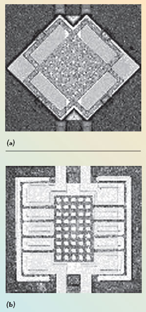
Fig. 6 Examples of bridge designs; (a) stiff and (b) less stiff.
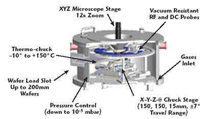
Fig. 7 Schematic picture of the MEMS test chamber (PAV).

Fig. 8 Change in capacitance versus time for the switch with a stiff bridge.
The switching speed is increased drastically if the device is operated at reduced pressure. Figure 9 shows the same device operated at 2 × 10⁻⁴ mbar N2. In this case, the pull-in and pull-out times are much shorter. In addition, however, a large overshoot effect causing a long settling time is observed when the bridge returns to the up-state (low capacitance). Because the device is not damped anymore when not touching the dielectric, it starts vibrating with a large amplitude (overshoot).11 Figure 10 shows a magnification of part of the signal measured when the bridge reaches the down-position. It is clear that even when going down and touching the dielectric, a vibration effect called bouncing can be observed. This effect has to be avoided and it is clear from the figures that an optimum pressure exists (critical damping), at which the bridge moves very fast, but no overshoot occurs when it moves back up. To experimentally obtain the optimum pressure, a successive approximation method was used. In this method, a pressure interval is determined in which the critical damping is located. This interval is divided in half by performing an experiment at the pressure in the middle of the interval. When overshoot occurs, the critical damping point is located in the higher pressure half of the interval, otherwise in the lower pressure half. The interval in which the critical damping point has been found to be located is cut in half again by performing another measurement, and so on, until the critical damping point has been accurately found. This method is very effective — high speed electronic analog-to-digital (A/D) converters use the same principle to accurately determine the value of a voltage.
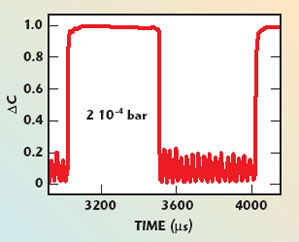
Fig. 9 Stiff bridge switch operated at low pressure.
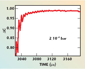
Fig. 10 Zoom-in of the pull-in time for the stiff bridge switch operated at low pressure.
Figures 11 and 12 show the results for the stiff and for the floppy bridge. Only the pull-out part of the DC versus time curve is shown, that is, when the bridge moves from the down position (large C) to the up position (small C). For both designs, there is a clear decrease in pull-out time with decreasing pressure. The stiff bridge does not show overshoot at 0.125 bar. At 0.075 bar, a small overshoot is visible, at 0.09 bar, no overshoot appears, while vacuum (2 × 10⁻⁴ mbar) results in a large overshoot. The switch with a less stiff design (switch B) and with a lower surface area shows overshoot already at 0.25 bar, as expected for a less-stiff switch. Not only the pressure inside the package, but also the gases inside the package cavity influence the MEMS. Figure 13 shows lifetime plots of capacitive switches. These measurements were also performed using the ELT system. The plots show the change in capacitance, ?C (in arbitrary units), between up- and down-state of the switch as a function of the number of cycles. Three switches from different origins and with different insulator material were tested. The first has SiO2 as the insulator, the second Ta2O5 and the last SiNx. For all switches, ?C stays rather constant for a certain number of cycles, and then suddenly drops. This ‘end-of-life’ is caused by the bridge sticking to the insulator; the bridge remains in the down-position. This is a well-known failure mode in capacitive RF-MEMS switches and is caused by a charge that builds up in the insulator when the switch bridge is touching the dielectric.12–16 The high voltage required to actuate the switch induces high electrical fields across the insulator, causing charge trapping. The experiments on these switches were performed at different switching frequencies, at different actuation voltages and on different designs, so the lifetime cannot be compared.16 The three switches were tested in normal (laboratory) air as environment, and, under the same actuation conditions, in nitrogen gas. For all three, the lifetime is clearly a factor of approximately 100 times longer in N2. These effects are attributed to the humidity of the air and its influence on charge trapping in the insulator.12
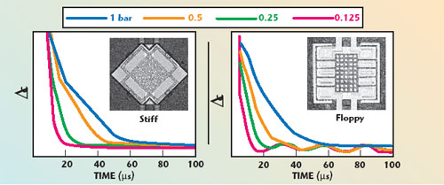
Fig. 11 Change in capacitance during down-to up-state at different pressures.
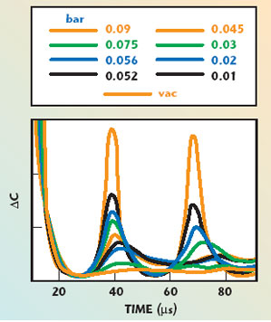
Fig. 12 Change in capacitance of the stiff switch after the transition from down-to upstate for different pressures.
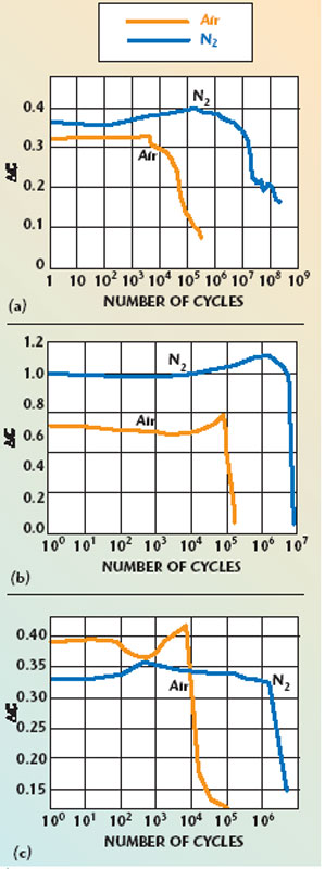
Fig. 13 Lifetime plots of three different capacitive switches in air and nitrogen environment with (a) SIOx, (b) TIO5 and (c) SINx insulators.
It is known that humidity enhances the charge trapping, leading to a faster charge build-up and, as is shown here, a shorter lifetime of the capacitive switches. It is interesting to note that for the three different oxides, the increase in lifetime when changing from normal laboratory air to nitrogen gas is very similar, whereas it is well known that these three different insulators have a rather different charge trapping sensitivity. This could indicate that these charging effects occur at the surface of the insulators. Another mechanism that could play a role is the difference in breakdown voltage of the small gap between the bridge and the insulator for the different environments. From these experiments, however, no clear conclusions can be made at this time. It is clear that additional research on these charging mechanisms in different environments is required. The charge typically disappears after some time. This effect is shown in Figure 14. First, a fast C-V experiment is performed. This is done using the ELT system by applying a triangular waveform to the switch instead of the normal unipolar square waveform to actuate the switch. The fast C-V principle is shown in Figure 15. During application of this triangular pulse, the change in capacitance is measured. The result is plotted in what are called fast C-V curves. The advantage of this measurement method is that it is very fast (~1 ms) compared to conventional C-V measurements (~1 min), so that only limited charge trapping takes place, which is, in general, not the case in conventional C-V measurements.

Fig. 14 Fast C-V measurements of a capacitive switch (a) before test, (b) after test and (c) 19 hours later.
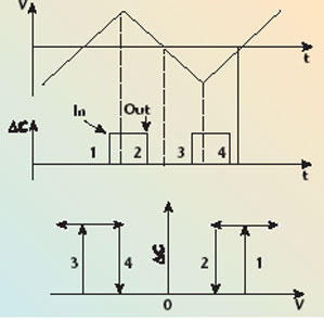
Fig. 15 Principle of the fast C-V measurement.
The results of a fast C-V measurement on a fresh switch are shown first. It is a symmetrical CV curve, showing clear pull-in (approximately ±22 V) and pull-out (approximately ±10 V). Next, a lifetime test is performed at a voltage (35 V) that is higher than the actuation voltage, until the failure of the switch. The results of a fast CV-curve, measured immediately after failure of this switch, are shown. The curve is clearly shifted to the right and is also narrower. The first observation is well known and modeled.13,14 It is caused by charging of the insulator, causing an increase in the pull-in voltage. The second effect is less well known but often observed in capacitive switches. It is caused by a non-uniform distribution of this charging.15 During this fast CV measurement, the switch is functioning and pulling in and out during the voltage ramp. In the ELT test, however, the switch is declared ‘failed’ because when switching fast from 35 V to 0 V, it will stay pulled-in.14 The results of a fast C-V measurement, performed on the same switch 19 hours later, are then shown. During that time, the switch was kept in a nitrogen environment. One clearly sees a partial recovering of the switch: the C-V curve is shifted back to the left and broadened again. This confirms that the charges decay in time and that this typical failure of capacitive RF-MEMS is not a permanent one. However, even after 19 hours, the charge did not disappear completely, indicating that these traps, whether they are surface or bulk, or holes or electrons, have a rather long decay time.
Conclusion
This article discussed some influences of the zero-level package on the performance of capacitive RF-MEMS switches. The influences of temperature, pressure and gases were discussed. The packaging process requires a certain temperature profile, which can affect the mechanical stress of the metal MEMS bridge. It is clear that when designing and processing an RF-MEMS, this effect has to be studied and taken into account to avoid that a good functioning RF-MEMS device will fail or change its functionality after being packaged. One of the main disadvantages of MEMS switches compared to, for instance, RF transistors and PIN-diodes, is their low switching speed.17 For many applications, a high switching speed is mandatory. In this article, it is shown that choosing a suitably low pressure, in combination with a well-selected device stiffness, can be used to optimize the switching speed of RF-MEMS switches. On the other hand, it is shown that a pressure that is too low can result in an anomalous vibration behavior for some MEMS. It is clear that for optimal performance, the devices have to be used in a zero-level package with an internal optimal pressure, or the design has to be adapted, depending on the desired speed for a certain application and on the environmental conditions (space versus earth applications). The first solution requires a constant, well-controlled pressure of the package; the second solution requires adapted MEMS designs taking into account application dependent functioning and reliability issues.
It is also shown that capacitive MEMS switches with SiOx, SiNx or Ta2O5 insulators exhibit a higher reliability when operated in N2 than in air. This is most likely related to enhanced charging of the insulator in the presence of humidity. Again these results influence the demands for the zero-level packaging of such switches. A fully hermetic package is likely to be required, and this hermeticity should be kept constant during the lifetime of the device.
Acknowledgments
Much of the material in this article was first presented at the 2005 IEEE International Reliability Physics Symposium and appeared in the Proceedings as “The Influence of the Package Environment on the Functioning and Reliability of RF-MEMS Switches” by W.M. van Spengen, et al., pp. 337–341. This work is supported by the European Union in the framework of the FP5 IST-28231 project MEMS2TUNE, the IST-28276 project MIPA and the FP6 NoE PATENT-DfMM.
References
1. H.A.C. Tilmans, W. De Raedt and E. Beyne, “MEMS for Wireless Communications: From MEMS Components to RF-MEMS-SIP,” Journal of Micromechanics and Microengineering, Vol. 13, No. 4, July 2003, pp. S139–S163.
2. R. Modlinski, A. Witvrouw, P. Ratchev, A. Jourdain, V. Simons, H.A.C. Tilmans, J. den Toonder, B. Puers and I. De Wolf, “Creep as a Reliability Problem in MEMS,” Microelectronics Reliability, Vol. 44: (9–11), 2004, pp. 1733–1738.
3. Y. Oya, A. Okubora, M. Van Spengen, P. Soussan, S. Stoukatch, X. Rottenberg, P. Ratchev, H.A.C. Tilmans, W. De Raedt, E. Beyne, P. De Moor, I. De Wolf and K. Baert, “A Reliable and Compact Polymer-based Package for Capacitive RF-MEMS Switches,” Proceedings of the International Electron Device Meeting, 2004, pp. 31–34.
4. A. Jourdain, P. De Moor, S. Pamidighantam and H.A.C. Tilmans, “Investigation of the Hermeticity of BCB-sealed Cavities for Housing (RF)-MEMS Devices,” Proceedings of MEMS2002, Las Vegas, NV, pp. 677–680.
5. P. De Moor, “The Minipackage: A Flexible Wafer-level Packaging Solution for MEMS,” Proceedings of the International Microelectronics and Packaging Society 6th Workshop on Packaging of MEMS, November 2004, Long Beach, CA.
6. H.A.C. Tilmans, H. Ziad, H. Jansen, O. Di Monaco, A. Jourdain, W. De Raedt, X. Rottenberg, E. De Backer, A. De Caussemaeker and K. Baert, “Wafer-level Packaged RF-MEMS Switches Fabricated in a CMOS Fabrication,” Proceedings of the International Electron Device Meeting 2001, Washington, DC, pp. 921–924.
7. A. Jourdain, H. Ziad, P. De Moor and H.A.C. Tilmans, “Wafer-scale 0-level Packaging of (RF)-MEMS Devices Using BCB,” Proceedings of DTIP 2003, 5–7 May, Cannes, France, pp. 239–244.
8. Veeco Instruments Inc., 100 Sunnyside Boulevard, Suite B, Woodbury, NY.
9. J.T.M. van Beek, M.H.W.M. van Delden, A. van Dijken, P. van Eerd, A.B.M. Jansman, A.L.A.M. Kemmeren, Th. G.S.M. Rijks, P.G. Steeneken, J. den Toonder, M.J.E. Ulenaers, A. den Dekker, P. Lok, N. Pulsford, F. van Straten, L. van Teeffelen, J. de Coster and R. Puers, “High-Q Integrated RF Passives and RF-MEMS on Silicon,” Material Research Society Symposium Proceedings, 2003, Vol. 783, pp. B3.1.1–B3.1.12.
10. W.M. van Spengen, R. Puers, R. Mertens and I. De Wolf, “A Low Frequency Electrical Test Set-up for the Reliability Assessment of Capacitive RF-MEMS Switches,” Journal of Micromechanics and Microengineering, Vol. 13, 2003, p. 604.
11. P.G. Steeneken, Th. G.S.M. Rijks, J.T.M. van Beek, M.J.E. Ulenaers, J. De Coster and R. Puers, “Dynamics and Squeeze Film Gas Damping of a Capacitive RF-MEMS Switch,” Journal of Micromechanics and Microengineering, Vol. 15, 2005, p. 176.
12. J. Wibbeler, G. Pfeifer and M. Hietschold, “Parasitic Charging of Dielectric Surfaces in Capacitive Microelectromechanical Systems (MEMS),” Sensors and Actuators A, Vol. 71, 1998, pp. 74–80.
13. W.M. van Spengen, R. Puers, R.P. Mertens and I. De Wolf, “A Comprehensive Model to Predict the Charging and Reliability of Capacitive RF-MEMS Switches,” Journal of Micromechanics and Microengineering, Vol. 14, 2004, pp. 514–521.
14. J.R. Reid, “Simulation and Measurement of Dielectric Charging in Electrostatically Actuated Capacitive Microwave Switches,” Technical Proceedings of the 2002 International Conference on Modeling and Simulation of Microsystems, Chapter 5: MEMS Applications and Characterization, 2002, pp. 250–253.
15. X. Rottenberg, B. Nauwelaers, W. De Raedt and H.A.C. Tilmans, “Distributed Dielectric Charging and its Impact on RF-MEMS Devices,” Proceedings of the 34th European Microwave Conference, 2004, pp. 77–80.
16. W.M. van Spengen, R. Puers, R. Mertens and I. De Wolf, Proceedings of the International Electron Devices Meeting, 2002, pp. 901–904.
17. J.J. Yao, “RF MEMS From a Device Perspective,” Journal of Micromechanics and Microengineering, Vol. 10, 2000, R9.
