
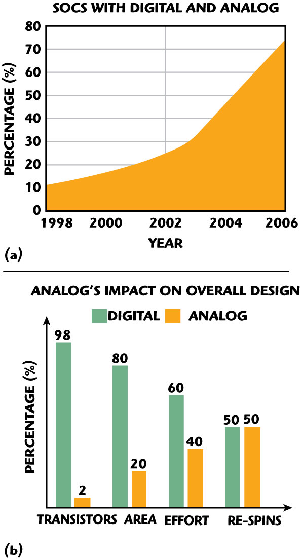
To address the space, cost and power-consumption constraints of mobile portable devices from cell phones to PDAs and laptops, the trend in RFIC design is to combine the analog baseband (BB) and processor interface into a single chip solution (see Figure 1). With new products experiencing narrow market-windows and shorter product life cycles, wireless applications are increasingly faced with the need to achieve “First Pass Functional Silicon.” Silicon re-spins that are most often due to functional errors on average cost $1 M for 90 nm and below.
Meanwhile, system demands on RFIC functionality, as multi-band and multi-mode operations, for example, further complicate this objective. In order to increase RFIC “functionality and features” while ensuring greater first-pass success, design organizations are adding new design skills, software tools and design data structures to their existing flows. In this article, the author discusses his first hand experience working with design organizations as they face the challenges of developing the models, simulation capability and automation that will accurately verify the behavior of a device operating across the RF to digital domains.
Digital-oriented A/MS to True Mixed-signal Functional Verification
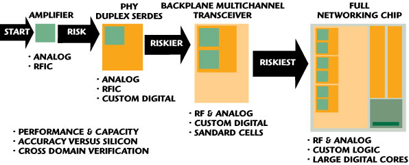
Advanced simulation capacity, model/design (silicon) accuracy and cross domain (time and frequency) capability are critical in addressing the engineering challenges associated with integrating analog, RFIC, custom digital and large digital cores (in system-on-chip) (SoC) designs (see Figure 2). A top-down design methodology, which includes block-level specification and compliance sign-off, strategically combined with full-chip functional verification for RF-A/MS (radio frequency and analog mixed-signal) applications can help to enable First Pass Performance silicon and is thus emerging as a necessary step before final tape-out. The concept of full-chip functional verification for RF-A/MS ICs is relatively new.
Today, many organizations developing SoCs are reviewing their existing digital IC functional verification methods as a guide for developing full-chip RF-A/MS functional verification within their wireless RFIC design environment. In prior years, (digital) functional verification teams would code transactional behavior for RF/analog/mixed-signal sections of an IC using digital behavioral languages such as Verilog or VHDL. This code (sometimes referred to as “dummy analog”) would provide a degree of block-to-block connectivity checking, modeled with some block-delay characteristics of the digital and analog interfaces (A/D and D/A converters). However, since true mixed-signal simulation and top-down design are not an integral part of this mixed-signal verification procedure, design errors at the mixed-signal interfaces quite often went undetected before the IC was fabricated and tested.
Digital functional verification teams also experienced a significant slow-down in their simulation times (or test suite execution) when analyzing analog/mixed-signal blocks that were represented with Verilog-A behavioral models as opposed to simple, less accurate transaction code such as Verilog or VHDL. This reduction in simulation speed is due to the greater number of data points required for a continuous-time analog simulation of Verilog-A models compared to a discrete time digital solver using Verilog or VHDL.
By containing the A/D and D/A interfaces within a model, mixed-signal behavioral languages such as Verilog-AMS and VHDL-AMS are able to provide excellent simulation efficiency with very accurate analog/ mixed-signal block behavior. The advent of mixed-signal simulators such as AMS Designer from Cadence and standardization of mixed-signal behavioral languages (Verilog-AMS and VHDL-AMS) opened the door for both RF to baseband, top-down design and full-chip functional verification (see Figure 3).
The demand for a full-chip functional verification methodology among RFIC (mostly RF/analog with a small amount of digital) and a/ms (complex, multi-million device radio and baseband) design groups is growing. Due to practical considerations, two distinct design verification methodologies have emerged depending on the focus of the design team. For RF-A/MS ICs with an emphasis on digital complexity, functional verification is being merged with digital verification CAD tools and methodologies (for example, assertion-based verification, coverage verification, et al.). In contrast, RF-A/MS ICs with little justification for dedicated digital verification will rely more on existing RFIC EDA tools and design methodologies for functional verification.
Model Development and Characteristics
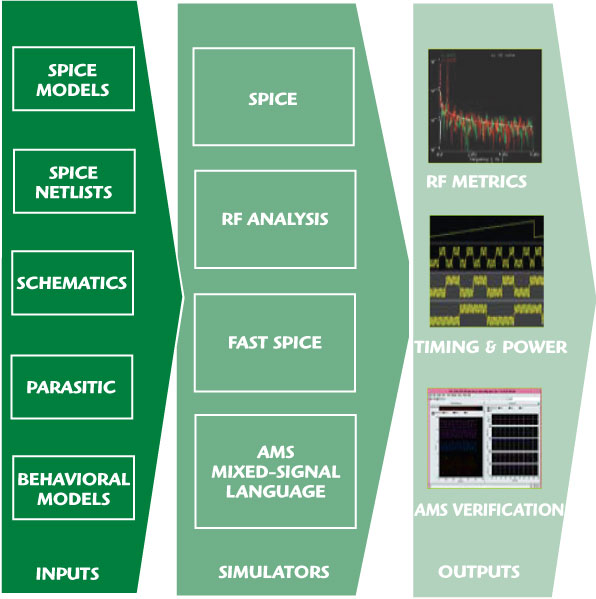
RFIC design groups utilizing true mixed-signal simulation technology as part of a top-down design methodology (system-level behavioral modeling) are generally better prepared to adopt a full-chip functional verification methodology. In addition to familiarity with top-down and bottom-up design process and practices, organizations with behavioral model language development and applicable model coding skills and established setup and characteristic simulation behavior of mixed-signal simulators will find it easier to implement RF-A/MS functional verification. Groups such as the IBM Silicon Solutions Engineering and IP Development team that are dealing with a broad range of designs every day, from high end foundry devices to memories, SERDES, standard cells, I/Os, cores and microprocessors have verification technology in place that is based on multi-mode simulation including circuit, RF analysis (PSS, transient and/or harmonic balance), Fast SPICE and A/MS simulation.
The primary technology enabler for RF-A/MS functional verification is a FVM (functional verification model) using languages: Verilog-A, Verilog-AMS or VHDL-AMS. As soon as chip-level definition, block-to-block integration, and block-boundary and pin definition is established, functional verification can begin.
The FVM development and testing process steps include:
• Developing block-level specifications for FVMs
• Developing FVMs and validating vs. circuit schematics
• Integrating and testing FVMs into various levels of hierarchy
• Performing full-chip functional verification
FVM Model Requirements
Before developing the model specification for functional verification, it is important to determine the component’s functionality as it relates to IC design complexity and which behaviors need to be simulated. If the design effort of the RF-A/MS IC is weighted toward the analog/mixed-signal, then it is highly probable that the FVM should contain “dual-functionality” in order to accommodate the following functional verification testing requirements:
1. FVM functionality should support the digital solver in order to perform fast simulations that are used to check for overall: power-up, supply, bias and clock distributions, chip state conditions from processor interface control (or on-board CPU control), etc. The FVM functionality for this type of verification test suite is termed “DC static functionality.”
2. As the IC database and block-designs become more complete, the FVM must support more time consuming tests to verify functionality of block-to-block signal quality transformation. Therefore, at the command-line the “signal quality functionality” of FVM can be selected for execution.
FVM specification for a block defines all the attributes for a given component with regard to its appearance in the design capture environment, electrical connectivity and behavior, and simulation control. It should be noted that the FVM specification is a dynamic document, but is typically frozen when the block boundary is frozen, which means block architecture in and around the block of interest is firm. The FVM Specification document is definitely frozen when FVM is validated against the circuit schematic.
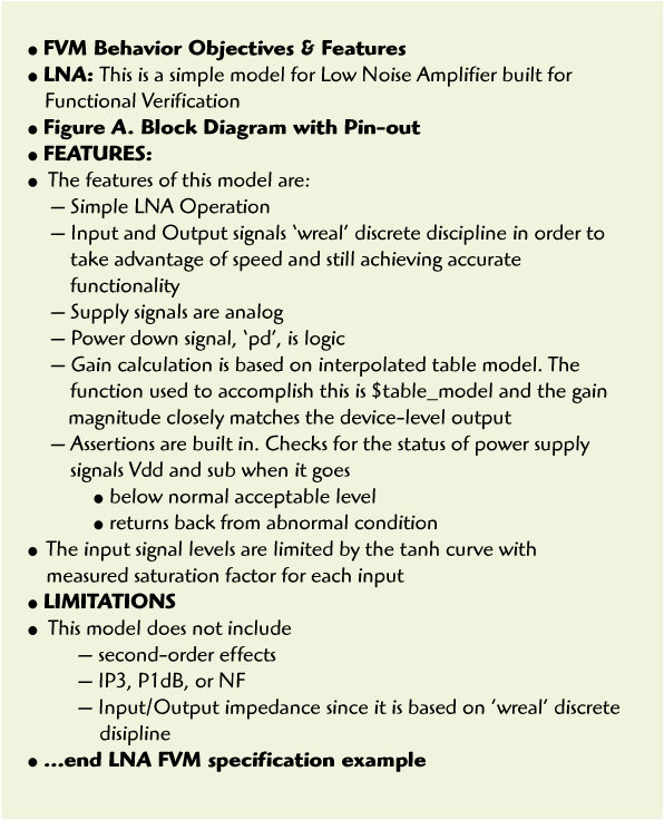
A typical block model includes a functional description, block diagram, specification table, Pin description table, assertion list and behavioral model objectives and features. An example of the behavior objectives and features for a FVM specification is shown in Figure 4. This FVM defines an LNA component that was used in an 802.11b/g IC design. The FVM is based on the Verilog-AMS language. The symbol for using the LNA in a top down design is shown in Figure 5. Since functional verification may involve a “suite” of tests to be performed, it is important to obtain accurate functionality and assertion behavior, while ensuring the fastest verification simulation throughput possible.
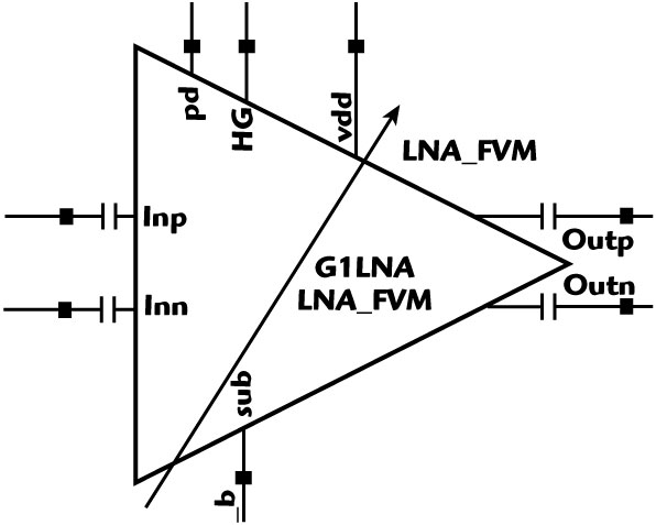
In this LNA block, the amplifier’s gain over the simulation range is a valid user parameter describing RF performance. In this particular model nonlinear effects (intermodulation distortion, IIP3 and power compression, P1dB) and noise parameters (NF) are not model parameters. However, this LNA FVM does include bias range as well as analog and digital control level specifications such as Vdd functional verification limits, Idd (sleep, standby, power-down and operational), input/output impedance: range-limits or “nominal” and analog and digital control levels/ranges. These are required specifications specifically for verifying block functionality.
To achieve both simulation speed and accuracy, it is imperative to use modeling techniques that take advantage of the particular behavioral modeling language being utilized and achieve optimum performance from the simulator. A good example can be seen with the above LNA example FVM. The use of the “wreal” function from the Verilog-AMS language allows the digital simulation solver to evaluate “wreal” (numeric value) change as a discrete event. This saves simulation time over the analog solver, which must use time-steps based on the period of the RF. For example: in an 802.11 b/g design, the RF period (1/2.45 GHz) divided by 20 or 40 samples required to achieve a smooth continuous time wave form leads to high sample rates (0.02 to 0.01 ps) and subsequent long simulation run times.
To ensure model accuracy the simulation results of the FVM must be consistent with those of the circuit schematic (fully modeled transistor-level IC design). The objective is to obtain a reasonable “signal quality” overlay of FVM and circuit schematic performance for a transient, periodic steady-state or harmonic-balance analysis simulation. Developing accurate performance from the FVM is a very important collaborative activity between the FVM modeler (sometimes from the Functional Verification Team) and the block design engineer.
Surprisingly, test benches created by FVM developers will often have more flexibility using behavioral models for stimuli blocks and measurement blocks than what a block design engineer may create at the circuit level. This type of FVM test bench is not only versatile and comprehensive, but also re-usable. Most block design engineers are encouraged to enhance their existing schematic-level test benches to accommodate the comprehensive test bench features defined in the FVM. However, since the block design engineer owns the final design, he/she usually does the FVM validation sign-off.
Sometimes even though the FVM validation has been “signed-off,” it is possible that insufficient functionality has been embedded within the FVM to fully demonstrate functionality at the top-level. For example: a radio (transmitter and receiver) based on a loop-back test bench configuration would require the ability to input the minimum number of symbols and frames into the transmitter and the ability to measure the EVM, BER and eye-diagrams on the output of the receiver for final functional quality test. An individual block designer may be unaware of all the required functionality testing at the system-level and thus leave this functionality out of the FVM. Therefore, entire design teams must work closely to develop FVM specification to ensure robust FVM blocks.
FVM Integration and Testing
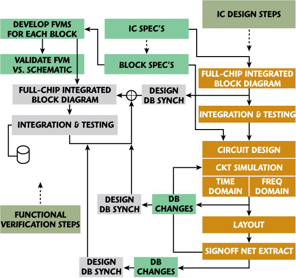
Functional verification testing is a constant on-going process, occurring interactively and in-parallel with the IC design process. The major objective of the on-going verification process is to constantly obtain a functionally correct IC database at the block-to-block, bond-pad-to-bond-pad levels. Verification test suites are typically run over night as a result of some design Engineering Change Order (ECO) that has occurred during the IC design process. Figure 6 presents a block diagram of the functional verification and design flow for an RF-A/MS IC.
The final quality of FVM functional performance is measured when all the FVM blocks (representing the various levels of IC hierarchy) are integrated to the full-chip level. Functional verification testing for the full-chip will typically be performed based on IC specifications. Therefore, the necessary stimuli will be supplied for all IC chip conditions and outputs observed and measured for expected results. Since full-chip functional verification is iterated throughout the IC design process, once an acceptable set of tests vs. output results are captured, then the testing can be converted to an automated compare process.
Full-chip Functionality at the Device/Component Level
With accurate FVM blocks in place, design groups are ready for full device-level functional verification/ simulation. Recently, new technology derived from RF simulation has been applied to device-level simulators such as Cadence’s Ultrasim and/or AMSUltra. These tools represent an evolution in the family of so-called “Fast Spice” simulators, which are necessary in order to maximize simulation throughput specifically for SoC with RF circuits. Instead of following the lead of SPICE simulators and solving a single large matrix, Fast SPICE partitions the circuit into many smaller stages. Each stage is solved as a single matrix, which results in speed-ups.
For RFICs, any blocks in the transmitter and receiver that are operating at high frequency represent potential bottlenecks for simulation throughput due to the “analog solver” and the small time-steps based upon a time-division of the smallest frequency period. Because of this, the best performance within a receiver and/or transmitter with standard “FastSpice” simulation historically has been in the range of 2x to 2.5x improvement over and above a standard SPICE analysis.
To meet the challenge of analyzing large device count circuit blocks, the next generation of Fast SPICE tools has been enhanced with “local Fast Envelope” analysis-mode capability. This feature can be applied “locally” to blocks of interest (RF blocks containing AM, PM, or FM modulation). This results in a 12 to 40 times simulation acceleration vs. SPICE simulation and removes the simulation throughput bottleneck. This large range of acceleration depends on verification objectives, that is, performance vs. functionality. Additionally, in device-level functional verification a higher speed can be obtained through lower accuracy settings, which may be an acceptable trade-off depending on performance-oriented verification requirements.

The Table 1 FVM and UltraSim Simulation Comparisons for an 8 ms simulation run is an example taken from Cadence’s RF Kit v5.2.1 for reference. Note that simulation throughput for using FVMs and using AMS Designer is listed.
Conclusion
IC design organization with experienced “digital-methods” functional verification team in place often set up automated functional verification tests at the beginning of the final design stages. However, very few RF-A/MS design organizations have a Functional Verification team (of the digital characteristic) actually performing true mixed-signal full-chip functional verification. Increased effort to develop automated verification testing among RF-A/MS IC design groups is expected as full-chip functional verification testing becomes a “simulation sign-off” requirement for tape-out.