GaN devices now operate at much higher bias conditions than traditional PHEMTs or HBTs, and also dissipate DC power and generate RF power at much higher densities.
Due to high RF and DC power levels, it was found that conventional CW device characterization and modeling techniques are no longer adequate. CW S-parameters, for example, are the basis for device model derivation used in empirical models as well as in data-based behavioral models.

For empirical model extraction, broadband CW S-parameters are used to extract equivalent circuit models and then to derive bias dependency of intrinsic parameters. For behavioral models, CW S-parameters are stored in a database and used directly for device simulation.
However, CW S-parameters are not easily measured for large devices, which cannot be biased safely to regions of RF trajectories under all drive levels and load lines without destroying these devices thermally. In this article, pulsed IV and pulsed S-parameter techniques are used to extract device models at high power levels.

It was found that some of the equivalent circuit parameters derived from pulsed S-parameters were very different from those derived from CW S-parameters. This discrepancy between CW and pulsed data was attributed to field-induced traps in the channel, affected by the quiescent bias conditions. For the highest power devices, however, the impedance level made it very difficult to obtain accurate S-parameters.
Here, it will be shown that a modified modeling and scaling process can be used where even the improved approach to device model extraction utilizing pulsed IV and pulsed S-parameters2 is no longer feasible.

An approach is demonstrated to model 100 W GaN HEMT devices, based on measurements of a 30 W device. The four types of devices investigated are commercially available GaN HEMTs from Eudyna Inc. with a total gate periphery of 11.25 (EG3001), 18.0 (EG4501), 27.0 (EG7001) and 36.0 mm (EG9001), respectively. They are capable of nominal output powers of 30, 45, 70 and 90 W, respectively, in the frequency band of DC to 5 GHz, although much higher saturated powers were obtained from each of them.
The largest device that could be characterized and modeled with acceptable accuracy was tested first. This was an EG3001 (30 W nominal) device. Pulsed IV and S-parameters were used to extract the large-signal model. The extracted model was verified against load-pull data under both single- and two-tone conditions.

Using the EG3001 model as the basis, the models for a family of GaN HEMT devices were scaled up, with the largest device (EG9001) demonstrating a saturated power up to 110 W at 2 GHz. The device simulation using these models agreed well with load-pull data under single- and two-tone drives.
MESFET Model for High Voltage Devices
A new model has been developed to accommodate the characteristics of high voltage GaN HEMT devices. Improvements were made to adequately represent the transition near the pinch-off region at high drain voltages. Excellent agreement is now shown with pulsed IV data up to 100 V.
The model can also be applied to lower voltage devices such as standard PHEMTs or enhancement mode devices with equally good results. The model is compliant with the charge conservation rule at gate and drain terminals.3 These improvements eliminated “non-physical currents,” resulting in much more accurate simulation of the device performance.

When the device is scaled to a larger periphery device, the channel temperature may not be the same as the original device. Thermal resistance for the scaled device may not share the same scaling factor due to the spreading of the heat flow. This may result in a higher channel temperature for the larger devices. Self-heating equations were implemented in the model, to enable adjustments to the change in the channel temperature. Figure 1 shows simulated IV characteristics with self-heating effects.
Characterization for Model Extraction
A family of four types of GaN HEMTs from Eudyna was characterized and modeled. The total gate periphery of these devices was 11.25 (EG3001), 18 (EG4501), 27 (EG7001) and 36 mm (EG9001), respectively. Each tested device was mounted on a chip carrier, which was then mounted in a test fixture.

The key data needed for model extraction include pulsed IV, S-parameters and load pull. There are challenges and limitations to this data acquisition due to high power conditions.
Pulsed IV
Pulsed IV data was taken to the limits of device thermal capability with a quiescent drain voltage of 50 V. With the largest device (EG9001), pulsed peak voltage of up to 100 V and current of up to 22 A have been tested. Figure 2 shows pulsed IV data of an EG9001 device, measured with Auriga’s AU4100 series pulsed IV system.4 The pulsed IV conditions were a pulse width of 2 μs and a duty cycle of 0.3 percent. The quiescent bias point was 50 V and 200 mA. Vg was varied between –15 and +2 V, in steps of 0.1 V.

S-parameters
Due to high power dissipation, these devices can only be safely DC biased at conditions near either the pinch-off or in the low drain bias voltage region. To extract parameters throughout the IV plane as covered by the RF trajectory under all power and load impedance conditions, pulsed bias becomes necessary to limit the instantaneous power consumption and minimize the temperature rise during the measurement.
In the pulsed S-parameter measurement system (see Figure 3), an Agilent pulsed network analyzer (PNA) was connected to the device to measure S-parameters while the device was pulse-biased using an Auriga pulsed IV system through a set of bias tees.

A complete set of S-parameters at 150 peak bias conditions for an EG3001 was measured and the equivalent circuit parameters were derived for all bias points.
S-parameter Dependency on Quiescent Bias Condition
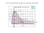
The bias condition has a strong influence on the performance of GaN HEMT devices, not only due to the thermal effect but also due to the traps populated in the channel. The electrical stress brought about by the bias voltages changes the channel and modulates the performance. This was observed in the pulsed IV data, when the quiescent bias point was varied. To test the bias dependency of S-parameters, two sets of S-parameters are measured, CW and pulse, as shown in Figure 4.
The CW set was chosen such that the device would be capable of thermally surviving the test. The CW set of S-parameters was taken with a 10 V DC bias on the drain and varying the gate voltage from pinch-off to Vgs = 0 V, shown by the black line in the figure.

The pulsed set was measured at the same instantaneous bias points as those in the CW test but with a quiescent bias condition fixed at 50 Vds, as shown by red arrows. Therefore, both data sets had the S-parameters taken at the same instantaneous bias point, with the only difference being that the pulsed data was quiescently biased at 50 V and the CW data was quiescently biased at the measured point (10 V).
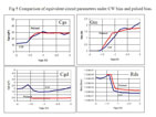
From the measured S-parameters, equivalent circuit models were derived and some intrinsic component values are compared in Figure 5.
Parameters such as Cgs, Gm and Cds were found to be similar in both CW and pulsed conditions. However, Cgd and Rds were found to be very different. This is because the difference in the quiescent bias conditions in these measurements (50 V in the pulsed measurement and 10 V in the CW measurement) is affecting the charge distribution in the channel.

This charge distribution, induced by the traps populated in the channel, has a slow time constant and is only affected by the quiescent bias condition. This shows the importance of pulsed S-parameter measurement and the limitation of CW S-parameters.
Limitation of S-parameter Measurements
For model extraction, low frequency data is used to determine the output conductance, transconductance and other parameters. As the size of the device increases, the conductance and capacitance also grow, resulting in very low device impedance.
The narrow frequency band of high current bias tees used to pulse-bias the device also makes it very difficult to measure low impedance levels at low frequencies.

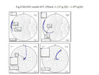
Figure 6 shows an example of pulsed S-parameters of an EG9001 (the largest in the family) GaN HEMT, the low end of the frequency band being limited at 0.5 GHz by the high current bias tee. As can be seen, the impedance is too low and the data does not have sufficient resolution to derive an accurate equivalent circuit.
Load Pull
The extracted large-signal model was verified against load-pull data. However, load-pull measurement of low impedance devices is as difficult as measuring S-parameters. The advantage of load pull compared to S-parameters is that load pull is usually performed at discrete frequency points while S-parameters are over a wide band from the lowest frequency point possible. For load-pull measurements, therefore, pre-matching circuits can be built for the frequency of interest directly at the input and output ports of the device, eliminating losses from long line effects or tuners.

The pre-matched load-pull fixture used for EG9001 model extraction is shown in Figure 7. A quarter-wave impedance transformer is built on a low loss Duroid board at 2 GHz. The pre-match circuits are characterized and their S-parameter blocks are derived for use in the simulation circuits.
Modeling of EG3001
An EG3001 (the smallest in the family with total gate periphery of 11.25 mm) was modeled based on pulsed IV and pulsed S-parameter data that was taken over a 0 to 100 Vds pulsed bias with a quiescent bias point at 50 Vds. The voltage dependency of these parameters is implemented in the Auriga MESFET large-signal model for high voltage devices discussed previously. The pulsed IV data is also modeled and implemented. The completed model is used to simulate small-signal and load-pull data. Figure 8 shows the simulated S-parameters at the operating bias point (50 V, 150 mA), compared to the pulsed S-parameter data. The comparison was made at a few other bias points, all resulting in good agreement. Figure 9 shows the single-tone and Figure 10 the two-tone intermodulation comparisons between the data and simulated results. Note that the device delivered a saturated power of 50 W, which was in good agreement with the simulated results. Agreements for gain, efficiency as well as for IM3 and IM5 were excellent.
Modeling of EG4501, EG7001 and EG9001
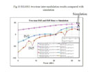
The devices EG4501, 7001 and 9001 are from the same family of devices as EG3001 with added cells to increase the output power, EG9001 being the largest with total gate periphery of 36 mm. As previously discussed, the model extraction from S-parameter data was not practical for these devices due to the resolution limitation of measured S-parameters. Large-signal models for all of these devices were derived from scaling the EG3001 model by the gate periphery ratio, 1.6, 2.4 and 3.6, respectively. All device parameters were scaled, except for the gate and drain inductances Lg and Ld, which were derived from matching the high frequency behavior of S-parameters. Figures 11 and 12 show an example of scaling applied to the largest device, EG9001. Single-tone and two-tone intermodulation data and simulated results are compared. Note that the device delivered a saturated power of 110 W, which was in good agreement with the simulated results. Agreement on its gain and efficiency, as well as IM3 and IM5 was also good over wide input power levels. The measured and simulated power (110 W) of EG9001 was less than the scaled power level expected from EG3001, which delivered 50 W. When the pre-matching fixture elements were replaced by ideal loss-less tuners in the simulation, the output power from the device increased by 1.5 dB, which agreed with the expected output power from a scaled device. This implies that the losses in the fixture contributed a loss of 1.5 dB in output power. The fixture loss becomes more critical for a device that presents very low impedance to the circuit.
Conclusion
The family of GaN HEMT devices, with output powers ranging from 50 to 110 W, was modeled successfully. The 50 W device (EG3001) model was extracted using pulsed IV and pulsed S-parameter data. Equivalent circuit parameters extracted from pulsed S-parameters revealed a strong bias dependency of these parameters, and demonstrated the importance of pulsed S-parameter measurement for model development. The EG3001 model was scaled in order to derive device models of larger devices up to EG9001 with power levels of 110 W. The model validity was verified by single- and two-tone load-pull measurements at 2 GHz. The scaling capability provides a successful approach to deriving models for 100 W level devices. This combined modeling and scaling approach provides the designer with a powerful and efficient tool.
Acknowledgment
The author would like to thank Eudyna Inc. for providing the devices and supporting this study. He also would like to thank Lou Pulzetti and David Wandrei of Auriga Measurement Systems LLC for measurement support.
References
- A. Maekawa, T. Yamamoto, E. Mitani and S. Sano, “A 500 W Push-pull AlGaN/GaN HEMT Amplifier for L-band High Power Applications,” 2006 IEEE MTT-S International Microwave Symposium Digest, pp. 722–725.
- J.P. Teyssier, P. Bouysse, Z. Ouarch, D. Barataud, T. Peyretaillade and R. Quere, “40 GHz/150 ns Versatile Pulse Measurement System for Microwave Transistor Isothermal Characterization,” IEEE Transactions on Microwave Theory and Techniques, Vol. 46, No. 12, December 1998, pp. 2043–2052.
- D. Root, “Modeling and Characterization of Microwave Devices and Packages,” 1999 Asia-Pacific Microwave Conference Workshop.
- AU4000 Auriga Measurement Systems.
Yusuke Tajima received his BS and PhD degrees in electronics engineering from Tokyo University in 1970 and 1980, respectively. He continued his research and development work at Toshiba Central Laboratories in Japan and then at Raytheon Research Division, which he joined in 1979. In 2000, he became the general manager of ACCO USA, responsible for the US operation of ACCO France. Since 2004, he has been the director of modeling and design for Auriga Measurement Systems LLC.
