
Although the temperature sensitivity of transistor parameters is significant for all types of power transistors, it is particularly important for the HBT, with its relatively poor thermal conductivity.
It is well known that the saturation currents and ideality factors of model diodes change with ambient temperature. This change has been fitted to exponential and polynomial functions in HBT models.2 However, if it is assumed that the saturation currents and ideality factors remain fixed at their ambient temperature values, their associated temperature dependence can be attributed to the increase of the base-emitter voltage by an incremental thermal voltage VTH.3 This is illustrated as follows:
where
Vbe0 = base-emitter voltage at ambient temperature T0
Pdsp = dissipated power in the device
Rth = thermal resistance
Determination of Thermal Resistance
The proposed method of determining thermal resistance uses forward Gummel measurements for different ambient temperatures and for different collector-emitter bias voltages Vce. This method was applied to an on-wafer 2 x 25 mm2 GaInP/GaAs HBT in a common-emitter configuration. The DC measurements were accomplished using a Cascade probe station, monitored by a program developed using HP-VEE software. A thermal chuck was used to set the ambient temperature of the device. MATLAB software was used for programming the extraction of the thermal resistance.
As proven by Zhang et al.,4 for a constant emitter current IE, the base-emitter voltage Vbe varies linearly with the junction temperature Tj. Thus, around an arbitrary temperature T1(T1≥T0), the voltage Vbe at temperature Tj can be written as
where
Vbe1 = base-emitter voltage at temperature T1
Knowing that Tj = T0 + RthPdsp, Equation 4 becomes
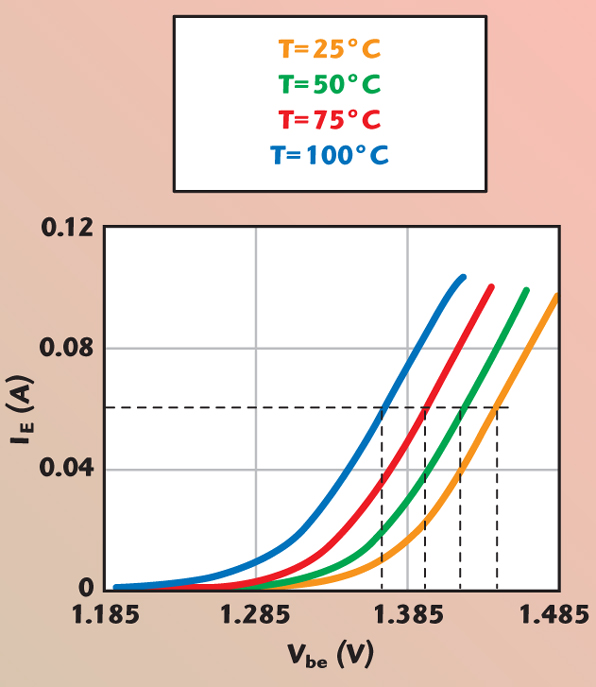
Two sets of measurements are necessary to determine the thermal resistance Rth. The first set of measurements contains the Gummel data at a fixed collector-emitter voltage of 1.5 V and variable ambient temperature (see Figure 1). The second set of measurements contains the Gummel data for a fixed ambient temperature (25°C) and a variable collector-emitter voltage. The extraction of the thermal resistance is illustrated in the following two steps:
Step 1
Considering the parameter P1 as the slope of the linear variation of the voltage Vbe versus the temperature T1 while the dissipated power Pdsp is maintained constant, as shown in Figure 2, one can write

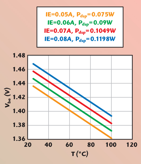
The dissipated power was calculated from: Pdsp = IcVce with Ic ª IE since Ic > 100Ib in the considered bias cases. The values of Ic and Vce were determined at a 25°C ambient temperature in each case, for the considered emitter current IE. In this first step, a set of values of the parameter

for different dissipated power is obtained.
Step 2
Considering the parameter P2 as the slope of the linear variation of the base-emitter voltage Vbe versus the dissipated power Pdsp (corresponding to a constant emitter current IE) while maintaining the temperature T1 constant, one can write

The dissipated power was calculated from Pdsp = IcVce with Ic ª IE.
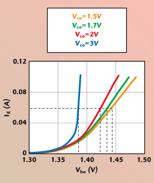
The values of Ic were determined at a 25°C ambient temperature in each case of the considered constant emitter current IE (see Figure 3). The collector-emitter voltage was fixed at 1.5 V. The values of the emitter current IE were the same as those considered in the first step. In this second step, a set of values of parameter

for different dissipated powers was obtained. The used values of the dissipated powers were the same as those determined in the first step.
Finally, using the values of parameters P2 and P1, the ratio P2/P1 was calculated, which allows for determination of the thermal resistance at each considered dissipated power Pdsp and emitter current IE

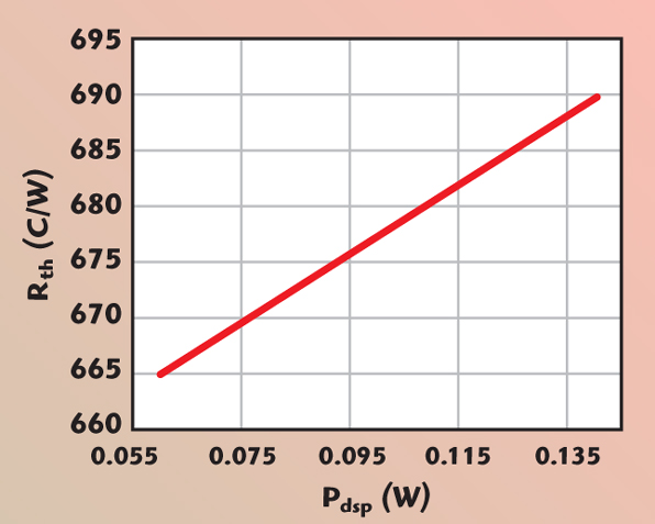
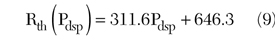
Experimental validation showed that the determined thermal resistance varies linearly versus the dissipated power. As shown in Figure 4, this variation is linear and can be calculated using the following derived formula
Inclusion of Thermal Effect in a HBT DC Model
The determined Rth was used to calculate dynamically the self-heating in a developed HBT DC model. A set of parameters for this model was determined, using methods reported previously.5,6 The proposed HBT DC model was implemented in the commercial simulator ADS as a symbolically defined device (SDD).
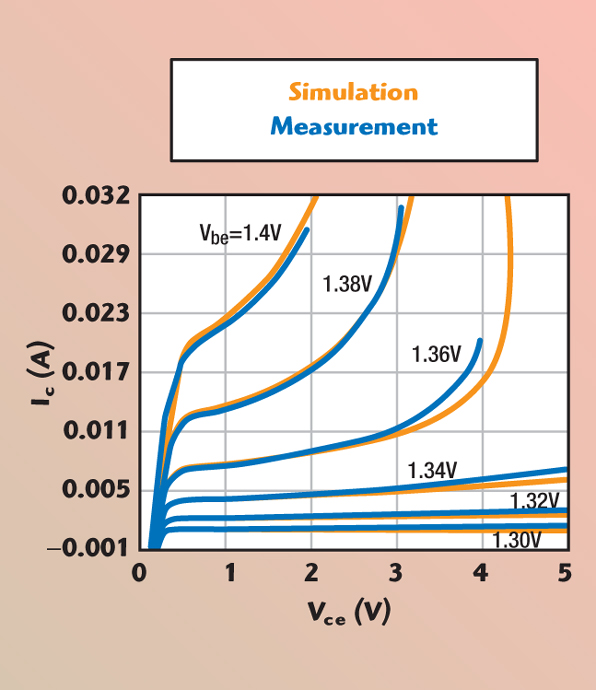
The implemented electro-thermal model has predicted accurately the DC characteristics of a 2 x 25 mm2 InGaP/GaAs HBT device, as shown in Figure 5.
Conclusion
A practical and detailed method for accurate determination of thermal resistance Rth and its power dependence was developed. This method used forward Gummel data at different ambient temperatures and at different collector-emitter bias voltages. The linearly power dependent thermal resistance was successfully used to calculate the junction temperature variation in a DC model of a 2 x 25 mm2 GaInP/GaAs HBT device. n
Acknowledgment
This research work was conducted as part of the author’s PhD studies at the PolyGrames Research Center, Ecole Polytechnique de Montreal, Quebec, Canada.
References
- P.M. Asbeck, M.C.F. Chang, J.A. Higgins, N.H. Sheng, G.J. Sullivan and K.C. Wang, “GaAlAs/GaAs Heterojunction Bipolar Transistors: Issues and Prospects for Application,” IEEE Transactions on Electron Devices, Vol. 36, No. 10, October 1989,
pp. 2032–2042. - C.T. Dikmen, N.S. Dogan and M.A. Osman, “DC Modeling and Characterization of AlGaAs/GaAs Heterojunction Bipolar Transistors for High Temperature Applications,” IEEE Journal of Solid-State Circuits, Vol. 29, No. 2, February 1994,
pp. 108–116. - Q.M. Zhang, H. Hu, J. Sitch, R.K. Surridge and J.M. Xu, “A New Large-signal HBT Model,” IEEE Transactions on Microwave Theory and Techniques, Vol. 44, No. 11, November 1996, pp. 2001–2009.
- D.E. Dawson, A.K. Gupta and M.L. Salib, “CW Measurement of HBT Thermal Resistance,” IEEE Transactions on Electron Devices, Vol. 39, No. 10, October 1992,
pp. 2235–2239. - S. Bousnina, P. Mandeville, A.B. Kouki, R. Surridge and F.M. Ghannouchi, “Direct Parameter-extraction Method for a HBT Small-signal Model,” IEEE Transactions on Microwave Theory and Techniques, Vol. 50, No. 2, February 2002, pp. 529–536.
- S. Bousnina, C. Falt, P. Mandeville, A.B. Kouki and F.M. Ghannouchi, “An Accurate On-wafer De-embedding Technique with Application to HBT Devices Characterization,” IEEE Transactions on Microwave Theory and Techniques, Vol. 50, No. 2, February 2002, pp. 420–424.
Sami Bousnina received his PhD degree in electrical engineering from the Ecole Polytechnique de Montreal, Quebec, Canada, in 2004. In 1999, he was an intern with Nortel Networks, Ottawa, Ontario, Canada, working on characterization and modeling of HBT devices. From 2004 to 2005, he was with Advanced Power Technology RF as a senior development engineer. He is currently a senior RF design engineer with M/A-COM, a division of Tyco Electronics, responsible for silicon bipolar device modeling and RF pulsed amplifier design.