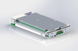
Figure 1 ADSY1100-series RF SoM.
System requirements are driving demand for compact electronic products with enhanced capabilities and shorter design cycles. The ADSY1100-series RF system-on-module (SoM) assemblies from Analog Devices, Inc. combine an RF tuner, sensors and a field-programmable gate array (FPGA) in a 3U VPX module aligned to the Sensor Open Systems Architecture™ (SOSA™) standard. The RF SoMs are available with swappable RF front-end mezzanine cards to provide a selection of frequency ranges from 10 MHz to 55 GHz. The small size, weight and power (SWaP) of these multifunction modules, coupled with selectable frequency ranges, help designers of advanced electronic systems in communications, electronic test and measurement, electronic warfare (EW) and radar systems to speed these devices to the production line. Figure 1 shows an ADSY1100-series RF SoM housed in 3U VPX enclosures with backplane connectors aligned to the SOSA™ standard.
The ADSY1100-series RF SoMs pack an RF/microwave tuner, Apollo MxFE® 20 GSPS high speed digitizer, microprocessor and a large FPGA into a single 1 in. pitch 3U VPX assembly. The system shown in Figure 1 features a slot profile for the backplane connectors aligned according to the SOSA™ standard. Within the compact VPX housing, the mezzanine cards connect to the heart of each digitizer, an Apollo MxFE™ model AD9084 signal converter housed in a ball grid array package. To sample signals from the RF tuner mezzanine cards, each AD9084 incorporates four 16-bit digital-to-analog converters capable of sample rates to 28 GSPS and four 12-bit analog-to-digital converters running at speeds up to 20 GSPS.

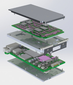
Figure 2 Rendering of the ADSY1100-series VPX module.
Marrying high dynamic range and wideband digitization with up to 10 GHz of instantaneous bandwidth with advanced processing capabilities in a reduced SWaP format, the AD9084 within each ADSY1100-series SoM feeds a Virtex™ UltraScale+™ VU11P FPGA from AMD connected to a Zynq™ UltraScale+ ZU4EG multiprocessor system-on-chip (MPSoC) device with 64-bit microprocessor capability from AMD Xilinx. These devices and the AD9084 signal converter are on the ADSY1100 Digitizer Base Card within each ADSY1100 VPX unit. The base card also houses optical transceivers, clock conditioning, power distribution and onboard memory. Multiple circuit cards fit within each ADSY1100-series VPX module, including a base card and an RF mezzanine card. Figure 2 shows a rendering of the components and the layout of the ADSY1100-series SoM.
The ADSY1100-series 3U VPX modules are well-suited for various applications, including wideband instrumentation, communications, radar and EW systems. This design is especially suitable for applications requiring reduced SWaP. The multiple-channel RF SoMs can be optimized and quickly deployed for a targeted frequency range by choosing swappable RF front-end mezzanine cards.
CHOOSING AN RF CARD
RF mezzanine cards are available for direct sampling in the 0.01 to 8.5 GHz and 0.1 to 18 GHz frequency ranges. They are also available for frequency tuning from 0.1 to 20 GHz and tuning input signals as high as 55 GHz. Each tuner card provides four receive and four transmit channels and operates on +3.3 VDC and +12 VDC power supplies.
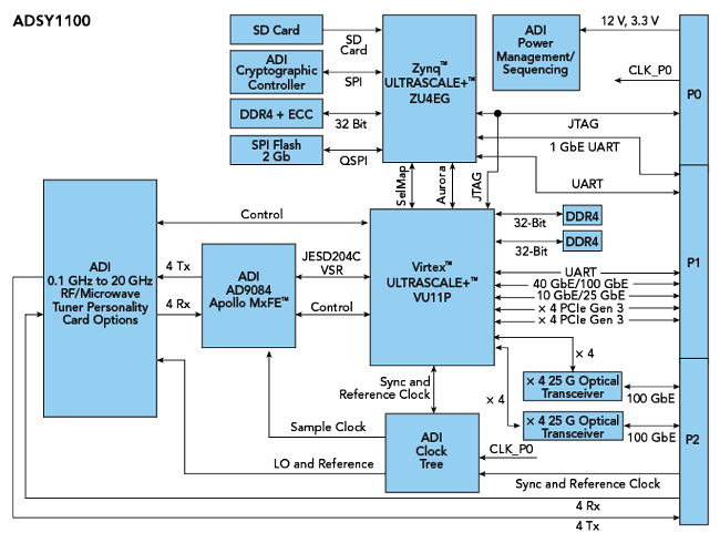
All ADSY1100-series SoMs offer an array of control interfaces, including 1, 10 and 40 Gb Ethernet, two-channel 100 Gb optical Ethernet and eight PCIe Gen. 3 connectivity lanes. Captured data can be stored within internal memory or transferred at high speed by the 100 Gb optical Ethernet port. The digitizers are protected against overvoltage transients and ESD, although ESD precautions should always be taken, given the high density of function and performance. Figure 3 is a block diagram of the ADSY1100-series SoM showing these functions and interfaces.

Figure 3 ADSY1100 functional block diagram.
THEORY OF OPERATION
The ADSY1100 Digitizer Base Card houses the AD9084, Virtex UltraScale+ FPGA and Zynq UltraScale+ MPSoC, as well as optical transceivers, onboard memory, a power distribution network, clock conditioning and more. The P0 and P1 backplane connectors connect directly to the ADSY1100 Digitizer Base Card to provide a 12 V power source, clock sources, auxiliary power, UART, JTAG, PCIe Gen3 data plane, 40/100 Gb Ethernet data plane, 10/25 Gb Ethernet data plane, 1 Gb Ethernet SGMII control plane, Aurora expansion plane and more. An onboard phase-locked loop/synthesizer accepts a low frequency reference clock. It synthesizes two 20 GHz output signals with low phase noise that serve as the sample clock for the AD9084 and the LO for some attached Tuner Personality Cards (TPCs).
A family of TPCs mates to the ADSY1100 Digitizer Base Card to enable optimized performance based on user case. Typical TPC functions include variable gain and attenuation, RF filtering, optional RF frequency conversion and switched paths. Among these, the 0.01 to 8.5 GHz personality card employs a simple RF chain to operate in the first Nyquist zone. However, a 0.1 to 18 GHz personality card implements a switchable filter bank for a higher frequency range to operate in the first and second Nyquist zones. A 0.1 to 20 GHz personality card uses an integrated up-converter and down-converter to operate in the first Nyquist zone for a different high frequency option. A pass-through personality card that omits the front-end signal chain to enable direct signal flow into the base card is also available. Detected and synthesized signals arrive on the ADSY1100 Digitizer Base Card via RF/microwave connectors delivered from the TPC.
Data is offloaded from the ADSY1100 Digitizer Base Card through a 2× 100 Gb Ethernet optical transceiver, which feeds P2A and P2B connectors or by storing the digitized data to onboard memory and subsequently querying the memory from the SGMII interface.
Analog Devices, Inc.Wilmington, Mass.
www.analog.com/adsy1100
