DIODE MEASUREMENTS, COMPLETE WITH WARNINGS
Unlike the DC I-V measurement described in Part 1 of this tutorial, measuring a diode’s OFF capacitance as a function of voltage is not straightforward. Many techniques can be used, from automated systems that determine the capacitance directly to the measurement of S-parameters via a vector network analyzer, which are then processed to determine the capacitance. While each technique has strengths and weaknesses, they all have issues that can creep up and lead to bad measurements. These issues may include:
- Poor calibration of the system; always check your calibration
- Incomplete de-embedding to the diode
- Measuring too small of a device, which allows parasitics to dominate the response
- Not measuring enough voltages, which can obscure the S-curve profile
- Poor layouts of MMIC devices that lead to inaccurate measurements
- Measuring MMIC devices on wafer with the microscope light on.
Of these, a MMIC with a poor layout can be the most frustrating, as overcoming these layout issues may require a separate fabrication run that will cost time and money. Unfortunately, diodes constructed as part of a foundry process control monitor tend to fall into this category and often cannot be used for capacitance extraction. Also, measuring a device with the microscope light on is the same issue described in Part 1, as external light can affect the diode’s capacitance. Once the challenges have been conquered and a good set of capacitance values versus diode voltage has been measured, it is time to extract parameters.
EXAMPLE 1: STANDARD PROFILE
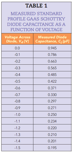
In this first example, a diode with a standard capacitance profile typically found in P-N and Schottky diodes fabricated on silicon, GaAs and GaN, with GaAs pHEMT the noted exception, is considered. Table 1 presents the measured capacitance for a GaAs Schottky diode fabricated on an obsolete commercial MESFET process.
The goal is to extract the three parameters in Equation 1, Cj0, Vj and m, from this measurement using the Solver function in Excel. This process is identical to that described in Part 14 and readers are referred to that article for additional details. To briefly explain the process, four sections are set up in Excel and these sections contain the capacitance parameters, the measured data, the modeled data and the root-mean-square (RMS) error. The following were chosen for seed values: Cj0 = 0.945 (the measured capacitance at Vd = 0), m = 0.5 (values between 0.3 and 1.0 are good starting points) and Vj = 0.5. The next step is to run Excel Solver with the goal of reducing the RMS error to zero. Figure 2 shows the results of this optimization with values for the desired parameters, Cj0, Vj and m, shown in cells C3, C4 and C5, respectively.
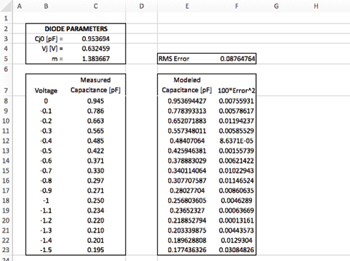
Figure 2 Standard profile GaAs Schottky diode results.
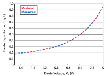
Figure 3 Comparison of measured versus modeled diode capacitance using the optimized parameters.
Solver has varied all three parameters from the seed values, generating a very low RMS error in cell F5. Note that in cells F8 to F23, the squared error at each voltage is multiplied by 100 to create larger numbers. Solver can fail when the target value is very small, so this problem is avoided by scaling up the squared error. The final values for these parameters are Cj0 = 0.954 pF, Vj = 0.632459 V and m = 1.383667. Figure 3 compares measured versus modeled capacitance using these optimized parameters.
Figure 3 shows very good agreement between measured and modeled results over the 1.5 V range. However, a well-known problem with Equation 1 is that as the diode voltage decreases further, the model can deviate noticeably from the measured data. For many diodes, the measured capacitance flattens out at these lower voltages and Equation 1 cannot accurately describe this behavior. Therefore, care must be taken if model accuracy is paramount at lower diode voltages. However, this discrepancy is not an issue in applications such as double-balanced mixers, since the diode ring will clip the diode voltage to levels where Equation 1 is extremely accurate.
EXAMPLE 2: S-CURVE PROFILE
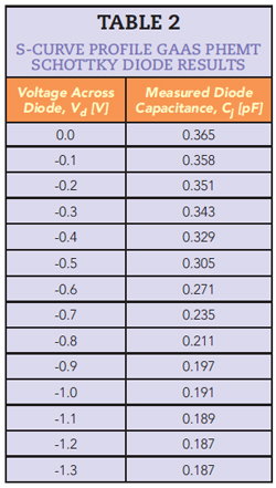
This second example will consider the more complicated S-curve capacitance profile. As mentioned earlier, Schottky diodes often generate this profile on many, but not all, GaAs pHEMT processes. Table 2 presents data from a diode fabricated on an obsolete commercial GaAs pHEMT process.
The goal is to use Solver to extract the seven parameters needed for the TOM model: Cgs0, Cgd0, Vbi, Vto, DELTA1, DELTA2 and Fc. The process is the same as in Example 1 but with some caveats regarding the seed values. While some parameters, such as Vto, can be negative, the TOM model works best when DELTA1 and DELTA2 are positive. Therefore, if the optimization results are negative for these parameters, the optimization process must be rerun with different seed values. In some circumstances, certain combinations of these seven parameters cause convergence problems when used in large signal/harmonic balance circuit simulation tools. If this happens, the situation can be improved by changing the seed values and rerunning Solver to generate new parameter values.
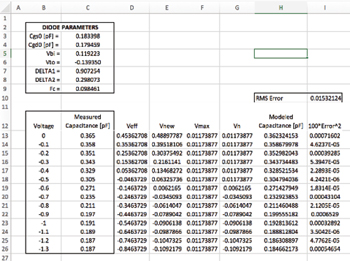
Figure 4 S-curve profile GaAs pHEMT Schottky diode results.
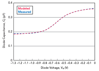
Figure 5 Comparison of measured versus modeled diode capacitance using the optimized parameters.
Figure 4 presents the results of running Solver. Extra columns are needed to compute the intermediate parameters Veff, Vnew, Vmax and Vn using Equations 2 to 5. Again, the squared error at each voltage is multiplied by 100 to generate larger numbers and a larger RMS error in cell I10, which helps convergence.
Figure 5 shows a comparison of the measured versus modeled capacitance profile. The curves show very good agreement between the measured and modeled results. This agreement would not be possible using the standard capacitance model of Equation 1. As with the standard profile, the TOM model tends to become inaccurate as the diode voltage gets lower, though the range of validity is generally greater than the standard model.
MODEL IMPLEMENTATION
The last step in this process is to implement the extracted parameters in a circuit model for simulation. This step is fairly straightforward. For example, Keysight’s ADS tool includes the DIODEM model block, which generates the standard capacitance profile and the TOM model block, which produces the S-curve capacitance profile. Additionally, both profiles can be programmed with the DC I-V parameters to complete the model. However, there are two caveats to note. First, some of the extracted model parameters scale with diode size, so they must be scaled for use in a general model where diode size remains a variable. Second, while the TOM model contains the saturation current, Is, as a variable, the extracted value from Part 1 of this tutorial must be halved when entered into the block. The TOM model assumes two parallel diodes in the FET, one from gate to drain and the other from gate to source. Creating a diode by shorting the drain to the source in the model will cause these two currents to add and generate the correct DC I-V response.
FINAL THOUGHTS
Diode modeling in Excel through the Solver function is a fast and efficient method for determining pertinent parameters. The process described in Parts 1 and 2 of this tutorial allows the engineer to control and understand the process, which is crucial. Proper modeling of the diode will lead to greater accuracy in circuit simulations. For example, the capacitance profile can affect intermodulation distortion in pHEMT diode mixers, so accounting for the S-curve is crucial for determining the third-order intercept point.
Finally, many subtle modeling aspects have not been considered in this tutorial. Among these are the effects of temperature on diode capacitance. If these parameters are important in the application, then techniques described in this tutorial can also be used to extract those parameters.
ACKNOWLEDGMENTS
A special thanks to John Mahon of MMIC Works for discussions on the TOM model and to Nick Novaris for checking the Excel calculations.
References
- R. Goyal, ed., High-Frequency Analog Integrated Circuit Design, New York: Wiley-Interscience, 1995, pp. 98–99.
- P. R. Gray and R. G. Meyer, Analysis and Design of Analog Integrated Circuits, New York: John Wiley & Sons, 1993, pp. 37–58.
- A. J. McCamant, G. D. McCormack and D. H. Smith, “An Improved GaAs MESFET model for SPICE,” IEEE Transactions on Microwave Theory and Techniques, Vol. 38, No. 6, June 1990, pp. 822–824.
- C. Trantanella, “Extracting Diode Parameters Using Optimization in Excel Part 1 – DC Parameters from I-V Measurements,” Microwave Journal, Vol. 67, No. 10, October 2024, pp. 68–76.

