Despite superior performance to solid-state technologies, RF MEMS devices have had almost no penetration in the RF front-end (RFFE) market during the last two decades. This is primarily because of direct or indirect mechanical challenges. These challenges give rise to reliability and packaging issues for the semiconductor industry. There are several solutions for RF MEMS packaging, but the consumer RF market is driven strongly by cost and these solutions are expensive compared to standard packaging techniques. Using nonstandard solutions leads to higher costs and hinders the volume production capability required for the consumer market.
Nanusens has focused on circumventing the challenges preventing RF MEMS technology RFFE adoption by the consumer market by implementing the technology on the back end of a standard complementary metal-oxide semiconductor (CMOS) process. This article introduces the Nanusens MEMS-inside-CMOS technology and subsequently presents an RF MEMS capacitive switch used as a digital tunable capacitor (DTC) building block. Electrical performance and reliability data will be presented to demonstrate a complete DTC prototype and its performance. An aperture antenna simulation compares the Nanusens MEMS-inside-CMOS DTC to a silicon on insulator (SOI) solution currently in the RFFE of some of today’s smartphones.
MEMS-INSIDE-CMOS TECHNOLOGY
Nanusens’ RF MEMS capacitive switches are implemented on the back-end-of-line (BEOL) of the CMOS process. The switches use the routing metal layers as structural components for the mechanical part and the inter-metal dielectric layers as the sacrificial material. Nanusens’ MEMS-inside-CMOS technology requires only one additional maskless step added to the standard CMOS fabrication process. This step, the inter-metal dielectric etching, allows the mechanical structure to move. The top metal acts as the lid of the MEMS cavity, with release holes distributed across the MEMS area. That allows the device to be sealed by standard re-passivation techniques on wafer-level chip scale packages. This method ensures low cost and the volume production capability of standard CMOS devices. These steps are shown in Figure 1.
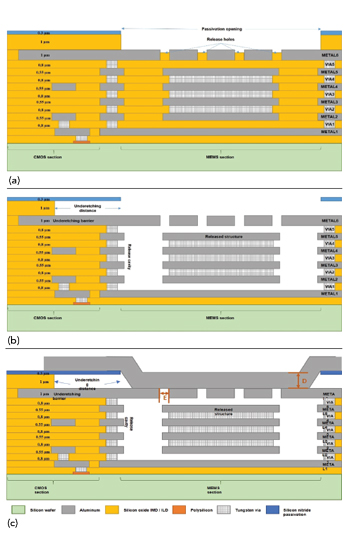
Figure 1 BEOL of the CMOS wafer after passivation opening (a). After post-processing etching (b). After sealing (c).

Figure 2 (a) COMSOL CMOS BEOL model to extract its residual stress. (b) Correlation between rotational displacement and residual stress. (c) SEM image of the residual stress test structure. (d) Confocal image of the residual stress test structure.
While the CMOS foundry can supply the electrical parameters of the BEOL layers, this is not the case for mechanical properties that are not applicable during ASIC circuit design. Nanusens has developed and implemented several test structures to obtain the necessary mechanical parameters like gradient and residual stresses and Young’s modulus to design these devices properly. Examples of these results are shown in Figures 2a to 2d.
However, the CMOS process is not intended as a MEMS process, so different design strategies and techniques were developed to overcome the limitations. RF MEMS capacitive switches have already been implemented and characterized in two different CMOS foundries (TSMC and SMIC) with similar performance. This demonstrates that the technology is compatible with mainstream CMOS foundries.
CAPACITIVE SWITCH DESCRIPTION AND PRINCIPLE OF ACTUATION
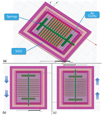
Figure 3 3D view of the capacitive switch model (a). ON-state gap (b). OFF-state gap (c).
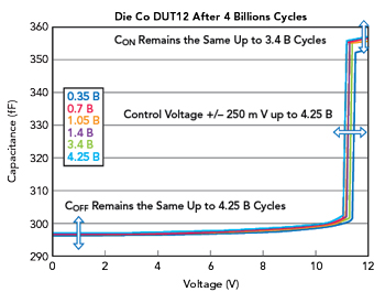
Figure 4 Switch C-V curve.
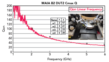
Figure 5 Switch Q.
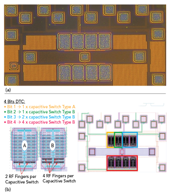
Figure 6 (a) Four-bit CMOS DTC prototype. (b) Capacitive switches used to implement the DTC.
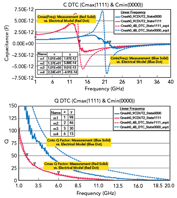
Figure 7 Measured and modeled capacitance and Q for 1111 and 0000 states.
The capacitive switch implemented with MEMS-inside-CMOS technology is a varactor that switches between ON and OFF capacitance states. It can be visualized as a binary capacitor with the ON state corresponding to a large capacitance value, while the OFF state corresponds to a low value. The device is implemented with an interdigitated structure shown in the ANSYS-HFSS© models of Figure 3. Figure 3a shows a 3D view of the capacitive switch model with stator fingers in orange and rotor fingers in green. Figure 3b shows the reduced stator/rotator gap in the ON state and Figure 3c shows the gap during the OFF state.
The device is enclosed in a MEMS cavity. It comprises of two parts not shown in Figure 3: the actuation section containing the actuation electrodes and the RF section containing the electrodes which exhibit the capacitance change between the two states. The DC circuitry is isolated from the RF components, ensuring no RF signal coupling to the DC. The actuation section generates electrostatic force by applying a control voltage between the movable and fixed electrodes to “pull in” the RF electrode, creating the ON state capacitance and “pull off” to achieve the OFF state capacitance. Pull-off electrodes ensure no self-actuation caused by large RF voltages when the device is OFF.
CAPACITIVE SWITCH RELIABILITY
The main failure mechanism of RF MEMS capacitive switches is dielectric charging due to charge trapping in the dielectric. This charge accumulation tends to generate an electrostatic force that can hold the device in the ON or the OFF state after removing the control voltage. Nanusens’ RF MEMS capacitive switches have no dielectric, ensuring that dielectric charging cannot cause failure. Taking advantage of the small gaps achievable with CMOS processes, the displacement of the movable part has been minimized to prevent failure due to the mechanical fatigue of the materials. ON/OFF state cycle testing has been performed by applying a 1 kHz square wave with a 50 percent duty cycle and the appropriate control voltage amplitude. Nanusens’ RF MEMS capacitive switches have survived more than 3 billion cycles without significant changes in their mechanical or electrical performance, demonstrating their suitability for antenna applications. Figure 4 shows the C-V curve with 11 V bias voltage.
These switches have been tested from -20°C to 150°C without noticeable performance degradation during operation. The switches have also been subjected to shock tests up to 6000 g and 50 Hz vibration tests for 30 minutes in each direction without performance degradation. They have also passed a preconditioning test, including 24 hours of baking at 150°C, seven days at 70°C/70 percent RH and six reflows up to 260°C for 15 minutes.
Currently, the main driver for yield is the etching post-processing step required to free the devices so they can move. Standard semiconductor equipment at the equipment manufacturer’s facilities does the etching step. Yield figures of 85 to 95 percent are constantly being achieved and the belief is that these will exceed 95 percent in production.
CAPACITIVE SWITCH PERFORMANCE
While dielectric-less capacitive switches prevent dielectric charging failure, the lack of a dielectric makes it more difficult to achieve large capacitance ratios. However, capacitance ratios from 2 to 4 are sufficient for aperture antenna applications in all bands from 0.5 to 6 GHz. These capacitive switches have capacitance ratios to 3.5, with the next generation of devices targeting a capacitance ratio of 5.
One of the main advantages of MEMS technology compared with solid-state technologies is the quality factor (Q). Some DTCs are currently implemented as SOI switches and off-chip capacitors. The ON state resistance of SOI switches is mainly determined by the channel resistance of the transistors (Ron). As the transistor channel length decreases, Ron decreases. While this increases the Q factor, it also reduces the breakdown voltage. This means stacking more SOI transistors to sustain the large peak voltage across the DTC, especially in aperture antenna applications. The series resistance of the transistor stack dominates the equivalent series resistance (ESR) of the SOI-based solution. There is a trade-off for SOI-based solutions among Q, power handling and area. The Nanusens switches have a Q of 190 at 1 GHz and 97 at 2 GHz, as shown in Figure 5. This is despite being implemented on a 10 Ω.cm resistivity standard CMOS silicon substrate. This is because the MEMS are enclosed in a grounded Faraday cage that prevents the coupling of the electromagnetic (EM) field into the lossy substrate. The maximum peak voltage the MEMS switches can currently withstand is 65 V in the OFF state and 50 V in the ON state. The next generation of capacitive switches will target 80 V peak voltage by improving the electrode robustness without degrading Q or increasing the area for a given capacitance.
Nanusens capacitive switches have high linearity. Measuring intermodulation distortion with tones at 875 MHz and 915 MHz gives an IIP3 value of 85 dBm, equal to the IIP3 of the unconnected setup. This indicates the IIP3 of the devices is greater than 85 dBm. The second-order harmonic distortion is also better than the setup, which measures -118 dBc. This linearity is due to the mechanical nature of the RF MEMS devices and the absence of dielectrics and semiconductor materials. The RF MEMS switch mechanical resonant frequency, which acts like a lowpass filter, is well below the RFFE RF frequency. Nanusens switches are also robust in front of low-frequency intermodulation distortion (IMD) products that can fall inside the mechanical bandwidth of the MEMS for some digital modulation schemes.1 This is because the switches are always in a well-defined position and held in place by large electrostatic forces. This prevents the device from responding to these signals within its mechanical bandwidth.
Current Nanusens RF MEMS capacitive switches have demonstrated that they can function up to 35 dBm without degradation. The in-house power handling setup is being improved to characterize the switches to 40 dBm.
Switching time depends on the stiffness and the actuation voltage of the switches. Depending on the application, the actuation voltage for Nanusens capacitive switches can be tailored to be from 5 to 100 V. Current variants with actuation voltages of 24 V have a switching time of less than 10 μs, which is sufficient for antenna tuning.
RF MEMS DTC
The RF MEMS capacitive switches can be arranged in an array to construct a DTC. Figure 6a shows the first prototype, which comprises an array of eight capacitive switches forming a four-bit DTC. Figure 6b details the capacitive switches used to implement the bits and their location in the DTC layout. Bit 1 comprises a single capacitive switch with one RF electrode. Bit 2 is also a single capacitive switch but contains two RF electrodes, doubling the capacitance. Bit 3 comprises two capacitive switches of the same type as Bit 2, while Bit 4 is implemented with four capacitive switches.
The dimensions of the DTC MEMS area are 360 μm × 400 μm for a maximum capacitance of 1.97 pF. The pad in the center part of the four-bit DTC shown in Figure 6a is the RF input signal with ground pads on either side for a shunt connection of the DTC. This creates a ground-signal-ground configuration with a 500 μm pitch. This prototype does not yet include the control electronics, so the capacitive switch control voltages must be applied through the pads around the die perimeter to switch the different bits to their respective ON and OFF state positions.
DTC PERFORMANCE
The prototype has been characterized to 20 GHz by measuring S-parameters. The capacitance ratio and Q have been extracted from the S11 measurements. The device has a capacitance ratio of nearly 2.2, from 0.9 pF when all switches are OFF to 1.97 pF when all are ON. The self-resonant frequency for the ON state is close to 13 GHz, demonstrating that the switch can be used for sub-6 GHz bands. The extracted Q is 50 at 2 GHz for the maximum capacitance state. These results are shown in Figure 7. The Q of the DTC prototype is less than the Q of the single capacitive switch. This is due to the routing parasitic resistance and requires optimization. FEM simulations with ANSYS-HFSS have shown that the routing resistance can be optimized to get a Q close to 100.
The DTC IMD has also been measured for the minimum (state 0) and the maximum (state 15) capacitance state using the same setup as for the capacitive switches. The DTC has shown an IIP3 better than 85 dBm for both states, corresponding to the unconnected IIP3 of the characterization setup. Furthermore, the second harmonic distortion of the 980 MHz fundamental tone has been measured at better than -118 dBc for both states at 40 V bias. This measured harmonic distortion corresponds to the unconnected characterization setup value.
The DTC prototype has been measured from -20°C to 100°C. It shows a 0.4 percent capacitance variation in the ON state and 0.1 percent in the OFF state. After device etch post-processing, the DTC shows a yield of over 85 percent.
APERTURE ANTENNA SIMULATIONS
Currently, DTCs for aperture antenna tuning are implemented with SOI xPxT/SPxT switches that require two to four off-chip components. These off-chip components increase the bill of material, cost and board footprint area. The off-chip components also increase parasitics, which could lead to unwanted resonances and increase design complexity. These solutions are limited by available off-chip component values and the tolerances for small values can be quite large, limiting the DTC resolution. MEMS-inside-CMOS DTCs are a single-die solution that reduces the board footprint by up to 30 percent compared to current solutions. They also minimize PCB parasitics, reduce design complexity and enable resolution to a few femtofarads.
To demonstrate the RF MEMS-inside-CMOS DTC performance advantages versus current SOI-based solutions, a tunable dual-band aperture antenna, based on the planar inverted-F antenna (PIFA) of a smartphone, was modeled using ANSYS-HFSS. Two different DTCs have been attached to the antenna to address low band (LB) 690 to 960 MHz and low mid band (LMB) 1420 to 1520 MHz frequencies. Simulations were performed using RLC values extracted from models and measurements of the MEMS DTCs and SOI 4P4T switches. S-parameters of off-chip capacitors have been obtained from vendor websites and board trace parasitics were not considered for the SOI-based solution.
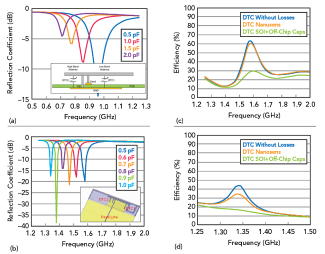
Figure 8 (a) LB performance. (b) LMB performance. (c) Antenna efficiency for the low-frequency range of LMB. (d) Antenna efficiency for the high-frequency range of LMB.
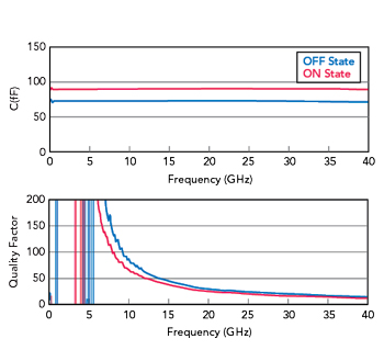
Figure 9 Capacitive switch capacitance and Q for the ON and OFF states.
A DTC with a capacitance ratio of 4 covers LB, as shown in Figure 8a. A capacitance ratio of 2 is enough to cover the LMB, as shown in Figure 8b. Figure 8c shows the antenna efficiency for the lower LMB frequency range and Figure 8d for the upper LMB frequency range. The antenna efficiency plots show results for both solutions and without DTCs. Antenna efficiency is improved in the LMB upper and lower ranges by 17 percent and 30 percent, respectively, using the MEMS DTC versus the SOI solution. Results for the LB, not shown, have antenna efficiency improving by 10 percent for the upper and lower parts of the band. This exercise has been repeated for the high mid band (HMB) in the 1710 to 2200 MHz range. In this case, the antenna efficiency improvement resulting from the RF MEMS DTC is 15 percent for the lower part of the band and 25 percent for the upper part. The antenna efficiency improvement is mainly due to the higher Q of the RF MEMS DTCs compared to SOI-based solutions. Further improvement in antenna efficiency of RF MEMS-based solutions could also improve ACPR due to increased linearity, especially using the high voltages that can be present on the DTC in aperture antenna applications.
Nanusens has recently demonstrated that its metal-air-metal (MAM) RF MEMS capacitive switch achieves a very high Q factor up to 40 GHz with a capacitance ratio of 2.5. This performance is shown in Figure 9. It should be noted that switch capacitance results are without de-embedding the pad capacitance estimated to be 60 fF and for frequencies less than 5 GHz, the resistance is close to zero.
CONCLUSION
Despite its superior performance, RF MEMS technology adoption in the RFFE market has been very slow compared to solid-state technologies. After many years of development, Nanusens has solved many challenges that have slowed adoption. Nanusens’ RF MEMS-inside-CMOS technology permits mass production and maintains production costs well below those of other MEMS solutions. The costs of these solutions can be below those of SOI switches while offering improved performance.
Nanusens DTCs can be easily implemented in antenna tuners, aperture antennas and reconfigurable matching networks on smartphone RFFEs for better and faster voice and data transmission. The technology’s advantages will also help reduce dropped calls and improve battery life by increasing antenna efficiency. The DTCs will be available as a 9-pin WLSCP with a 350 μm profile and expected dimensions of 1.5 mm x 1.5 mm.
The Nanusens RF MEMS-inside-CMOS DTC can be integrated with control electronics and ESD protection at the die level. This allows area and cost savings compared to system on chip and multi-component solutions. The DTC will be fully compatible with 2G/3G/4G/5G power handling and linearity requirements and it provides a MIPI RFFE interface for configuration and control. It enables a viable choice for future 6G solutions, especially in microwave bands.
References
- A. Lázaro, D. Girbau and L. Pradell, “Distortion Produced by RF MEMS Varactors on Digital Communication Signals,” Microwave and Optical Technology Letters, Vol. 48, No. 2, Feb. 2006.

