Concerning lights being on during measurements, this is a potential issue with on-wafer measurements of diodes because a microscope light is often needed to align the wafer probes. It is very common to leave the light on or, as often happens, forget to turn the light off during the subsequent I-V measurement. However, in most applications, the semiconductor diode will be packaged in some manner and can operate in the dark. The presence of light can affect the performance of the diode as compared to operation in the dark, so make sure to handle external light appropriately when performing a measurement. Once those problems have been conquered and voltage versus current measurements have been obtained for your diode, it is time to determine n, Is and Rs.
PARAMETER EXTRACTION THROUGH EXCEL OPTIMIZATION
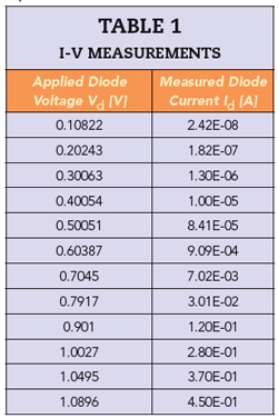
The optimization process is demonstrated through an example. Table 1 shows the I-V measurements of the 1N4148, a workhorse silicon diode first manufactured in 1960 that is still in use today.
Note that the measurements start at 0.1 V since the leakage current begins to appear below this range. Since Equation 4 cannot model the leakage current, this data must be ignored to obtain a good fit for the equation. It could be argued that this is not a valid approach because seemingly important data is being ignored. However, as discussed earlier, this leakage current will have little to no effect on diode behavior in the overall circuit in most situations. In addition, Table 1 is only a subset of the data offered by 2N9304blog.com, with additional data reduced for illustrative purposes. In practice, an I-V measurement would likely include more data points over the operating range.
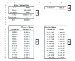
Figure 1 Excel spreadsheet with measured versus modeled diode parameters.
The next step is to move to Excel and set up the optimization problem. Figure 1 presents the data section of an example spreadsheet with section numbers added to aid in the description.
The spreadsheet is broken down into four sections to understand the process better:
Section 1: Cells C2, C4 and C5 contain the diode parameters, n, Rs and Is, to be determined. In a slight twist, the saturation current, Is, will not be used in the optimization; rather, it will be its natural log, ln(Is), placed in cell C3. Unfortunately, optimization routines in Excel can fail when the parameters have vastly different magnitudes. This problem is avoided by taking the natural log of Is and generating a number of the same order of magnitude as n and Rs. These values must also be seeded for the optimization to work. Values of n = 1.0, ln(Is) = -22 and Rs = 2.0 Ω are chosen as the seed values. These seed values work best when reasonably close to the expected result. Finally, cell C6 contains the temperature at which the diode was measured. This temperature is then used to calculate β in cell C7 using Equation 3.
Section 2: Cells B11 to B22 contain the applied voltage, Vd, and cells C11 to C22 contain the measured current, Id. These values are the measured data from Table 1.
Section 3: Cells E11 to E22 contain the calculated value of diode voltage, Vd, based on the measured current and the relevant parameters using Equation 4. This may seem counterintuitive since the measurement was most likely performed by applying a diode voltage and measuring the current. Now, the measured current is being used to develop a model for the diode voltage. However, as mentioned earlier, this approach works best given the nature of Equation 4, where the voltage across the diode can be determined by the current through it.
Equation 5 is entered into Excel cell E11 to set up the model. This can then be copied to cells E12 to E22:

Finally, in cells F11 to F22, the squared difference between the modeled voltage in Column E and the applied voltage in Column B is computed.
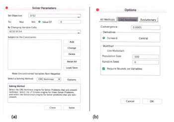
Figure 2 (a) Solver function initial menu. (b) Solver function Options menu.
Section 4: Cell F2 contains the root-mean-square (RMS) error of the data contained in cells F11 to F22. This single number is used to drive the optimization engine.
With the measured and modeled data now set up in the spreadsheet, the next step involves the Excel Solver function. This function is located under the “Tools” menu but can be enabled using the “Excel Add-Ins” function if it does not appear. Installation instructions for this function are readily available in the Excel Help section and online. The goal is to have the Solver function vary the parameters in cells C2, C3 and C4 to bring the RMS error in cell F2 as close to zero as possible. Figure 2a shows the initial Solver function menu and Figure 2b shows the Solver function options, along with the initial values that are entered to start the optimization process.
In Figure 2a, the Objective cell, F2, is set to a value of zero rather than choosing “Min.” This is done because the Solver function performs better with a specific numerical goal. Next, uncheck the “Make Unconstrained Variables Non-Negative” box since ln(Is) will be a negative number. If this box is left checked, the optimization will fail. The “Select a Solving Method” box is the optimization engine. Choose “GRG Nonlinear” and keep all the associated options at their default values of convergence = 0.0001 and population size = 100, as shown in Figure 2b.
Figure 3 shows the updated spreadsheet results after running the Solver function.
From the results, the Solver function has varied n, ln(Is) and Rs from the seed values to generate an RMS error below 0.005. The final values for our parameters are: n = 1.85219, Is = 2.62748e-09 and Rs = 0.40865 Ω.
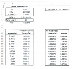
Figure 3 Solver function results for the diode parameters in cells C2, C3 and C4.
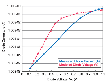
Figure 4 Comparison of measured versus modeled DC I-V curve using the initial seed parameters.
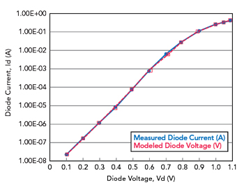
Figure 5 Comparison of measured versus modeled DC I-V curve using the final optimized parameters.
Figure 4 shows the measured versus modeled results for the initial comparison using the seed values for the diode parameters. Figure 5 shows the measured versus modeled comparison using the final optimized values. Both figures use a logarithmic scale on the y-axis for diode current to aid in visualization. We note that the Solver function has found a very acceptable solution in Figure 5, as the modeled result is a near-perfect match to the measured data, especially at the upper end of the voltage range.
FINAL THOUGHTS
After the diode parameters have been extracted, the results can be compared to published values or a DC model may be created for use in a circuit simulation tool. However, there is a note of caution regarding the modeling of Schottky GaN diodes constructed from field-effect transistors. These diodes often have an inflection point in their DC I-V curve at a voltage level near the turn-on point, defined as the point where the diode current is 1 mA. While the reasons for this phenomenon are beyond the scope of this article,3 such behavior in GaN diodes invalidates the Shockley model in Equation 1, so it cannot be used to model the DC I-V characteristic.
To complete the diode model, the OFF capacitance must be considered. The approach to determining the parameters associated with this capacitance is similar to what the article has presented. However, there is an added difficulty since the OFF capacitance can take on one of two distinct patterns and most commercial circuit simulation tools can only handle one type of relationship in their diode models. This phenomenon and subsequent modeling of the OFF capacitance will be discussed in Part 2 of this tutorial.
References
- R. Goyal, (ed.), “High-Frequency Analog Integrated Circuit Design,” New York: Wiley- Interscience, 1995, pp. 98–99.
- S. Stobbe, “1N4148 Diode Forward Biased I-V Curve,” 2N3904Blog, October 11, 2017, Web: https://2n3904blog.com/1n4148-diode-forward-biased-i-v-curve/.
- K. Hyeon Baik, “Design Fabrication, and Characterization of Gallium Nitride High Power Rectifiers,” Ph. D. diss., University of Florida, 2004, pp. 47–57.

