GUIDELINES ON ROUTING MULTIPLE RF TRACES
Designing PCB traces for RF beamformers with multiple RF inputs and outputs is difficult. As described, careful choice and design of the transmission line topology is required. In addition, correct ground via fencing into the device is important for good return loss and isolation. The isolation requirement and the geometries of the BFIC drive the transmission line topology decision. For example, GCPW is a good choice if the isolation needs to be around - 40 dB. If it needs to be approximately - 65 dB, based on experimental results stripline transmission lines are required.
Next, consider the geometry of the BFIC, focusing on the size of each pin, the pin-to-pin pitch and the distance between RF pins. For example, consider a BGA with a solder ball diameter of 5.5 mil (0.22 mm), 10 mil (0.4 mm) pin-to-pin pitch and 30 mil (1.2 mm) between RF pins with an isolation requirement of - 65 dB. A good choice for this scenario would be symmetrical stripline with approximate dimensions of 6 mil line width, 6 mil thick dielectric (above and below the line) and a 10 mil lateral gap-to-ground, assuming a dielectric constant in the low threes. The rule of thumb for stripline is to have a lateral gap-to-ground distance approximately twice that of the line width since smaller gap distances start to affect line impedances. Smaller distances between RF pins require a thinner width, while larger distances between RF pins accommodate a wider line. The latter is preferable since it provides a higher chance of attaining 50 Ω in manufacturing.
ROUTING NEAR THE DEVICE

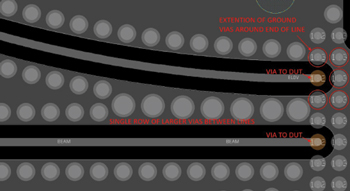
Figure 6 Ground wall vias extending around the transmission line.

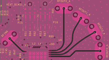
Figure 7 Fanout of multiple RF outputs.
When using stripline, care must be taken when transitioning to the device pin on the top layer, as this transition can degrade the isolation significantly if appropriate grounding vias are not used. To attain the highest isolation, the ground wall of vias should extend around the end of the stripline at the device transition, as shown in Figure 6 . This technique extends the critical ground wall required for best isolation performance. The device should also have ground pins, bumps and/or a ground paddle that surrounds the signal pin and should roughly coincide with the extended ground wall vias.
RF pins located a short distance from each other may not provide enough area for each transmission line to maintain its same via fencing into the device. Depending on the available area, the typical options for the via fencing are:
- Use smaller vias if they do not violate the fabricator’s aspect ratio rules for the dielectric thickness
- Stagger the vias in a sawtooth pattern where there is a moderate amount of area if the absence of a via on one of the lines at the device interface will not degrade isolation
- Use a single row of larger size vias between the lines while maintaining the same distance between the edges as the smaller via holes to optimize isolation performance, as shown in Figure 6
- Use a single row of same-sized vias when space between the lines is very limited.
The decision of when and how to fanout traces depends on where the RF I/O pins are in relation to each other on the device. The general rule of thumb is that fanout should happen as soon as it is feasible to reduce parallel runs, which maximizes isolation. As seen in Figure 6, the fanout can happen immediately because of the RF pin positions. However, Figure 7 shows the fanout of different parallel run distances of four outputs. In this case, the fanout is constrained by the non-RF I/O routing and associated circuitry shown on the top side of the device (L2, L4, P15, P16, etc.) and the RF outputs on the right side of the device.
INTRA-BOARD CONNECTIONS
RF impedance discontinuities between RF transmission lines and the RF connectors are as important as the trace-to-device transition. When transitioning between boards, there are two physical interconnect options:
- Edge launch connectors that mount laterally onto the edge of the PCB
- Vertical launch connectors that mount vertically onto the PCB.

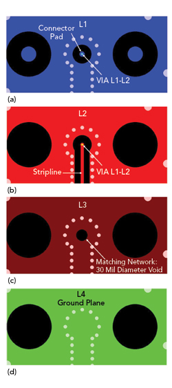
Figure 8 (a) Layer 1 ground plane, pad and via. (b) Layer 2 stripline. (c) Layer 3 30 mil void matching network. (d) Layer 4 solid ground plane.
Both types are available in SMA, SMP, SMPM, 2.92 mm and 2.4 mm interfaces.
The equipment form factor strongly influences the choice of edge launch versus vertical launch connector. Edge launch connectors imply laterally-arranged interconnecting PCBs. This arrangement may be the best choice if the system sits in a single metal chassis/heat sink. Vertically launched connectors offer the possibility of stacking multiple boards. This may result in a more compact form factor but this configuration may also require air cooling since the individual boards are unlikely to have heat sinks. A combination of one board having an edge launch while the other has a vertical launch results in the boards connecting orthogonally in a slotted style.
While edge launch connectors are widely used, they have potential drawbacks stemming from being attached at the board edge. Edge connectors require that the top ground plane of the PCB and, preferably, the bottom ground plane extend to the board’s edge. Most PCB fabricators can only guarantee a 2 mil distance between the edge of the ground plane and the board’s edge at the connector locations when using standard edge milling/routing and etch pullback techniques. This manifests as an impedance discontinuity due to the lack of ground return in the 2 mil, or larger, gap and degrades the return loss.
Because they are not bound to a board edge, vertical launch connectors are not susceptible to these edge routing issues. On simple, single-device boards, the connectors can be placed close to the device to minimize insertion loss. In addition, the transition onto the board can be matched so that impedance discontinuities are minimized. Some connector vendors will create a custom footprint for a given line design and stack up. Figure 8 shows four PCB layers for an SV Microwave vertical launch connector interface to a stripline RF trace.
One challenge of vertical launch connectors is achieving good alignment between the connector and the PCB footprint during assembly. Ideally, the connector’s circular center pin connects to its circular pad on the PCB with the centers aligned. However, left-to-right and forward-to-back movement is possible when mounting the connector on the 2D ground plane. Movement in either of these two directions will cause the center pin to be misaligned with the PCB pad. The best alignment method is a tight tolerance on the mounting hole size to minimize the movement of the connector.
CONCLUSION
Modern, high frequency BFICs are making PCB design more challenging. To maintain high channel-to-channel isolation, some RF trace designs are forced to migrate from surface-level GCPW to buried stripline. Even when using buried stripline, care must be taken to maintain isolation between adjacent traces using closely spaced via fencing that fully encircles the device’s pins. When approaching these challenging designs, PCB designers can preempt potential manufacturing problems by avoiding very thin RF traces or designing the characteristic impedance slightly below the target value. When designing board-to-board interconnects, top launch or edge launch interconnects will most likely be chosen based on the form factor of the end equipment. Top launch interconnects are less susceptible to manufacturing limitations at the board’s edge.
References
- J. Coonrod, “Comparing Microstrip and Grounded Coplanar Waveguides,” Rogers Corporation, Web: https://rogerscorp.com/blog/2020/comparing-microstrip-and-grounded-coplanar-waveguides.
- “PCB Tolerances in Fabrication,” MADPCB, Web: https://madpcb.com/tolerances/.
- “Tolerances,” AdvancedPCB, Web: https://www.4pcb.com/pcb-design-specifications.
- “PCB Fabrication Tolerances,” Imagineering, Inc., Web: https://www.pcbnet.com/capabilities/fabrication/tolerances/.
- “Stripline,” Microwaves101, Web: https://www.microwaves101.com/encyclopedias/stripline.
