The signal-to-noise ratio (SNR) is the primary noise characterization parameter for analog-to-digital converters (ADCs). The three main contributors to SNR performance are quantization noise, thermal noise and clock jitter. While most of these parameters are inherent to the device, the clock jitter performance contribution from an external clock can be controlled by the user. This article will provide calculations to predict overall SNR performance from measured clock phase noise sweeps and show practical techniques to achieve the best performance when operating with high frequency clocks for RF sampling converters.
Introduction
High-end communication and radar systems require a clock source with very low phase noise for data converters. SNR specification characterizes the noise performance of an ADC. A higher SNR translates to a device with a better opportunity to detect a small signal in the presence of noise. A good clock is vital to getting the best performance from the data converter.
Noise Contributions
ADC noise comes from three core elements: quantization noise, thermal noise and clock jitter. Each element contributes to the overall SNR performance, as shown in Equation 1:

Where:
SNRT = Total SNR
SNRQ = Quantization SNR
SNRN = Thermal noise SNR from the number of bits (N)
SNRj = Jitter SNR
Quantization Noise
The ADC resolution (number of bits) determines the quantization noise. Equation 2 shows the standard SNR calculation for quantization noise based on the number of bits, N:

Where:
SNRQ = Quantization SNR
N = Number of bits
High-end radar systems or communication systems use high speed data converters sampling at over 1 GSPS. These converters are typically 12 or 14 bits. Per the standard equation, the quantization noise of a 14-bit converter is about 86 dB, which is usually two orders of magnitude better than the remaining factors in practical devices. As such, you can ignore the quantization noise contribution.
Thermal Noise
ADCs have an underlying thermal noise component, but the device’s datasheet does not explicitly specify that parameter. Instead, it is best to use the published SNR performance data at very low input frequencies, 10 MHz, for example, to gauge the thermal noise contribution. At very low input frequencies, the clock jitter component has minimal impact, so thermal noise is the dominant factor. Noise output is proportional to signal output amplitude, and the convention is to measure from 1 to 3 dB below the full-scale output.
Clock Phase Noise
The SNR contribution from the clock, expressed by Equation 3, depends on the clock jitter and input frequency but not the clocking frequency:

Where:
SNRj = Jitter SNR
fin = Input frequency
τj = Clock jitter

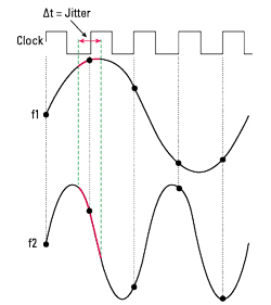
Figure 1 SNR impact related to input frequency.

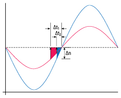
Figure 2 Benefits of a high slew rate clock.
It is a bit counterintuitive to realize that it does not matter how fast a device is clocked. When thinking about high-sampling speed converters, what matters most is the speed or frequency of the input signal. Figure 1 illustrates this concept. For a given amount of clock jitter, the variation in the crossover points where an actual sample is taken creates more error from ideal on a faster-moving, higher frequency signal than a slower, lower frequency signal. There is an indirect relationship to sampling speed because designers typically use high-sampling converters to pass high bandwidth, high frequency signals. As such, clock jitter performance is an important performance metric.
Slew Rate Impact on Jitter Performance
Ideally, the clock signal would be a perfect square wave, as depicted in textbooks. A perfect square wave represents an infinite slew rate of a clock transition from low to high. This is not possible with real-world clock signals because of bandwidth limitations. High frequency clocks are generally pure sine waves.
Assume that the ADC samples the signal at the zero-crossing of a clock pulse. Traditional timing jitter is the random variation of a clock with respect to time. This means that zero-crossings occur at a slightly different offset location from the ideal location. Thermal noise on the clock produces an equivalent effect because it generates random fluctuations in the amplitude of the signal. As the clock signal approaches the zero-crossing, a sufficiently high amplitude fluctuation causes the sample to trigger slightly prematurely.
A low-amplitude sinusoid clock approaches the zero-crossing at a relatively shallow angle, representing a low slew rate and is more susceptible to thermal noise impacting jitter. By increasing the amplitude of the clock, the transition becomes steeper. Accordingly, an equivalent thermal noise fluctuation on the higher slew rate clock translates to a lower timing error. This is shown in Figure 2, where the signal with the higher slew rate undergoes a smaller timing error versus a lower slew rate signal in the presence of the same thermal noise fluctuation (Δn). The takeaway is to drive the clock inputs to the ADC hard, on the order of 10 to 15 dBm, to keep the slew rate as sharp as possible.
Measuring Clock Jitter
The clock jitter comprises two components: aperture jitter and sample clock jitter. Aperture jitter is the contribution from the ADC device itself within its clock distribution circuitry. This parameter is extracted directly from the device’s datasheet. Sample clock jitter comes from the external clock source. The total clock jitter is the root mean square sum of each component, as expressed by Equation 4:

Where:
τj = Total clock jitter
τa = Aperture jitter
τClk = Sample clock jitter
Sample clock jitter is not a parameter that is readily provided. It is calculated from the clock source’s phase noise performance. Equation 5 expresses the clock noise by integrating the phase noise performance (L(f)) over the desired frequency limits:

Where:
NClk = Clock noise
L(f) = Phase noise (dBc)
The integration limits for Equation 5 depend on the application. The start frequency, f1, should be the location where the information is important. If using the information to estimate the error vector magnitude (EVM) of a communication signal, the best choice would be to start integrating on the lowest subcarrier frequency, which is usually a few kilohertz. For adjacent channel power ratio measurement calculations, the best choice might be to start near the frequency edge of the signal, which may be several megahertz. The final frequency, f2, should be set to the maximum signal bandwidth or the maximum measured frequency offset if the instrument limits are below the maximum signal bandwidth.
Equation 6 shows the jitter calculated from the clock noise at a specific frequency of operation:

Where:
τClk = Clock jitter
NClk = Clock noise
fClk = Clock frequency
The factor of 2 in Equation 6 accounts for converting the single-sideband (SSB) phase noise analyzer measurement to a full double-sideband (DSB) parameter. Theoretically, the clock jitter should remain constant. When doubling the frequency, the phase noise should ideally become 6 dB worse, indicating that it doubles as well. In practice, other contributions come into play as the frequency is modified, so an actual measurement is prudent for the best accuracy.
Example Calculations
As an example, the following analysis measures clock phase noise performance and estimates the corresponding ADC SNR performance. The ADC device is a Texas Instruments ADC32RF45 operating in decimate-by-4 mode with an external clock at 2457.6 MHz. The input frequency is 1.75 GHz, operating at -3 dBFS. Assume that the SNR from thermal noise is 65 dBFS, derived from the low frequency performance of the ADC in the datasheet.
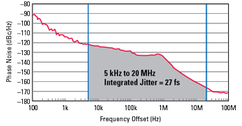
Figure 3 shows the phase noise measurement of the clock source. The phase noise integration lower limit is set to 5 kHz, which is roughly the smallest bin size in the ADC capture fast Fourier transform (FFT) plot. The high end of integration is set at 20 MHz, which is near the maximum of the instrument. Within the limits of integration, the clock jitter is 27 fs. From the ADC device data sheet, the aperture jitter is 70 fs. The composite clock jitter from Equation 4 is about 75 fs. Note that the external clock jitter is quite good and contributes only a slight increase over the device’s aperture jitter in this case.

Figure 3 Clock phase noise and jitter measurement.

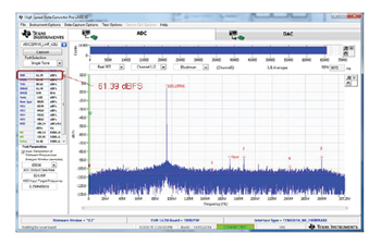
Figure 4 ADC32RF45 FFT capture and SNR measurement.
The SNR from the composite clock jitter is about 61.7 dBc at the desired input frequency. The next step is to adjust the value for the given carrier level to get a clock SNR of 64.7 dBFS. Next, combine the SNR from the clock with the SNR attributed to thermal performance from Equation 1 to get a composite SNR performance of 61.8 dBFS. Figure 4 shows the actual FFT measurement under this condition, where the reported SNR performance is 61.4 dBFS. The calculations match the measured results within a few tenths.
Conclusion
Most of the parameters affecting a data converter’s SNR performance are set for a given device, but a user can influence the choice of the data converter clock. Maintaining the best clock phase noise performance leads to the best performance from the device. The jitter calculations assist in cascading clock performance to an overall data converter SNR performance to ensure that system specifications are met.
