MADE-TO-ORDER LAMINATES
Laminates are used extensively in microwave and mmWave circuits. The applications of these laminates range from simple microstrip patch antennas to complex multi-layer stack-ups. Besides application and performance specifications, choosing a laminate often begins with dielectric constant (Dk).

Figure 1 Laminates can have different dielectric constants, panel thicknesses and copper claddings.
Laminates with a Dk value in the range of 2 to 4 are widely available, with selective commercial availability up to a Dk value of 13. The laminate’s thickness, another design factor that affects RF performance, is generally limited to a handful of options. But what if you could specify laminate Dk, thickness and copper cladding according to your precise requirements? With more variables under your control, fewer design tradeoffs and compromises would be needed to maximize bandwidth, reduce size and weight or improve gain. Figure 1 shows three laminates with different dielectric constants, panel thicknesses and copper claddings from WavePro.
CUSTOMIZATION OPTIONS
WavePro® ceramic-filled PTFE laminates are manufactured to your specifications. Available as standard 24 in. × 18 in. flat panels, the following parameters can be customized:
Dk: from 2.0 to 20.4 (in increments of 0.1)
Panel thickness: 1.5, 2, 4, 8 and 10 mm
Cladding: electrodeposited or rolled copper foil, 0.5/1/2 oz., surface roughness LP/VLP/ULP.
Laminates are manufactured locally at our facility located in New York. Lead times may vary depending on the laminate specifications and order quantity.
THE FOUNDATION: A HIGH-QUALITY DIELECTRIC MATERIAL
Due to its low loss and excellent dielectric properties, high purity PTFE is the basis for WavePro dielectric materials. Ceramic fillers are added to the host PTFE matrix to control the dielectric constant, loss tangent and coefficient of thermal expansion of the composite material. The formulation of fillers varies, as one ceramic may be used to enhance or mitigate the effects of another. Formulations are calibrated to maintain consistency within and between production batches.
Testing and characterizing the material’s dielectric properties is essential to the quality assurance process. WavePro products are tested to the following industry standards:
- ASTM D2520: cavity resonator method for unclad dielectrics
- IPC-TM-650-2.5.5.5: stripline method for laminates
- Free space transmittance/reflectance: techniques for mmWave/THz frequencies.
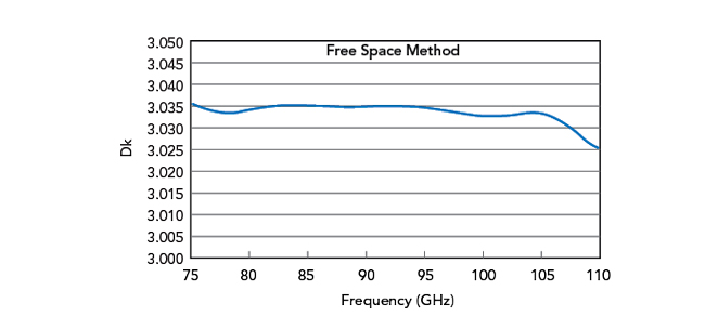
High purity ingredients, precise formulations and a stringent quality assurance process yield an engineered dielectric with reliable, stable properties. Figure 2 shows the variation of the dielectric constant with frequency for WP030 (Dk = 3.03 at 5 GHz). Even at 110 GHz, the Dk is within 0.2 percent of its nominal value.

Figure 2 Substrate dielectric constant, 75 to 110 GHz (WP030).
HIGH DK, THICK LAMINATES

Figure 3 Spiral Wi-Fi extender antenna.

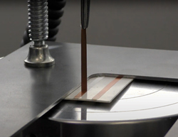
Figure 4 Copper peel strength test.
The custom manufacturing process for WavePro allows the production of laminate panels up to 10 mm (0.394 in.) thick, with a dielectric constant of up to 20.4. Miniaturization is one key driver for the use of high Dk laminates. As Dk increases, the wavelength decreases. Since many passive components are dimensioned to one-quarter or one-half the operating frequency wavelength, this effect can be leveraged to design hardware with reduced size and weight. Ultra-high Dk materials also exhibit increased capacitance, which benefits power integrity.
One limitation of traditional microstrip antenna elements is their narrow bandwidth. As wideband designs grow in demand, the use of thicker substrates will help overcome bandwidth limitations. However, as substrate thickness approaches or exceeds the electrical wavelength, care must be taken to avoid the excitation of higher-order modes. Figure 3 shows an example of a spiral Wi-Fi extender antenna fabricated with WavePro laminate material.
FABRICATION PROCESS
Custom laminates are manufactured using a two-step process. First, the unclad dielectric panel is fabricated to the specified Dk and thickness. The substrate is then placed between the specified copper foils (i.e., dual-cladded) and fusion bonded at high temperature and pressure. Proper adhesion of the copper foil to the dielectric substrate is essential, especially when the laminate undergoes multiple high temperature heating cycles during processing. WavePro custom laminates are tested following the IPC-TM-650-2.4.8 methodology. Results indicate an average copper peel strength of 16.0 lbs./in. for very low profile (VLP) copper foil. A photograph showing an example of the IPC-TM-650-2.4.8 copper peel strength test is shown in Figure 4.
OPTIMAL RF DESIGNS
WavePro custom laminates offer two distinct advantages for RF and antenna designers:
- Customized panels manufactured to specifications. This enables the adaptation of existing designs for performance optimization
- Extended range for high Dk (up to 20.4) and panel thickness (up to 10 mm). This enables new designs previously unattainable with laminates and potential space and weight reductions.
About WavePro
WavePro is a brand of Garlock, a manufacturer specializing in engineered materials and products with a history dating back over 130 years. Visit WaveProAntenna.com to request free samples and learn more about our laminates, unclad dielectrics and material specifications.
WavePro®
A Garlock Brand
WaveProAntenna.com
