While mobile communications claim the traditional sub-6 GHz bands and hungrily expand in the low mmWave region as they strive for higher data rates, lower latency and ubiquitous communications, other applications are shifting higher in frequency, beyond the conventional 40 GHz bands, as a consequence. The E-Band region (70 to 90 GHz) is being commercially populated primarily by terrestrial and satellite communications leveraging multi-GHz channels in that band.1 To further expand the available bandwidth, W-Band (90 to 110 GHz) and D-Band (110 to 175 GHz) are the natural evolution and commercial interest in these bands comes mainly from terrestrial communications.2 Wireless fronthaul and backhaul links are seeing timely and cost-effective deployments for mobile networks. The need for N × 10 Gbit/s data rates constantly pushes the envelope of regulatory limits and technological bounds.
The nature of 100 GHz signals implies substantial integration of the radio front-end. This is a key aspect determining the final performance. MMICs, used to implement the active RF functions,3 must be interconnected to low-loss distribution networks and antennas, often in waveguide technology.4

Figure 1 Integrating a MMIC and waveguide passive circuits.

Figure 2 3D cross-section of the proposed transition.

Figure 3 Waveguide matching adapter for the transition.

Figure 4 (a) Transition top view. (b) Close-up of feed.

Figure 5 Full-wave transition simulations.
This article proposes a transition between a coplanar waveguide (CPW) that might be used to integrate a MMIC and a rectangular waveguide, as shown in Figure 1. In industrial applications, such transitions entail specific requirements and desired features that must align with standard fabrication and assembly procedures. A key requirement is reducing design complexity while maintaining versatility. The proposed transition configuration meets both criteria, utilizing a single-layer printed circuit board (PCB) that can accommodate four different feeding arrangements to simplify the design and enhance adaptability.
TRANSITION DESIGN
Requirements and State-of-the-Art
The design concept is based on three requirements:
- The transition must be low cost and have the broadest operating band that does not require an external back-short
- The transition design must be hermetic and compatible with standard PCB assembly, which implies a final washing
- The interconnection should match a waveguide section and 50 Ω coplanar transmission line by exploiting a single dielectric layer compatible with thin-film technology.
Existing solutions proposed in the literature address only some of these requirements. Some citations5-7 require a multi-part custom waveguide structure, while others8-10 involve an undesirable back-short component or suffer from radiation loss. To meet all the requirements, the proposed design is based on a single layer of AD996 Superstrate alumina from Coorstek Inc. with a nominal thickness of 0.005 in. The thin-film carrier substrate has outstanding electrical performance, especially in the mmWave range11 and is physically stable.12
The integration concept is represented in Figure 1. The MMIC is placed on the top layer of the alumina circuit and wire bonded to a 50 Ω grounded coplanar waveguide (GCPW). Then, the signal is routed into a hollow metallic waveguide to exploit its intrinsic high quality factor. For D-Band, the standard is the WR-06, which nominally operates from 110 to 170 GHz and features a 1.651 mm × 0.8255 mm rectangular section.
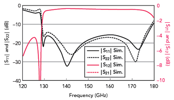
The transition must work from 130 to 175 GHz in this case, implying a 29.5 percent bandwidth. Return loss must be better than 15 dB, while the insertion loss must be a maximum of 1 dB. In addition, eliminating the need for an external back-short and fully sealing the transition are attractive features.
Since the ceramic dielectric constant is nominally 9.9, an embedded quarter-wavelength back-short can be embedded in the 0.005 in.-thick substrate without any aperture cut. To complete the impedance matching, a stepped tapered-waveguide transformer is implemented. This structure, shown in Figure 2, facilitates the transition between the air-filled waveguide and the high-permittivity substrate.
Layout
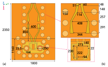
The transition involves a single alumina dielectric layer with top and bottom thin-film metal layers. The metal stack-up uses sputtered titanium and palladium, along with 3 µm galvanic-growth gold cladding. The resulting transition is 1.80 mm × 1.16 mm.
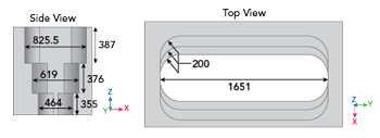
The operational principle is closely related to a standard microstrip-to-waveguide launcher. However, several design features improve the performance, add features and adapt the design to this basic stack-up. As shown in Figure 2, the design starts with the standard WR-06 waveguide transition. The standard waveguide interface allows the transition to interface with third-party devices and measurement instrumentation. The waveguide stepped transformer guarantees sufficient optimization capabilities. Figure 2 shows the two-step taper, implemented with rounded edges having a 0.2 mm radius as a by-product of CNC machining.
Figure 3 shows a lateral and top view of the detailed design with the optimized dimensions in micrometers. The S-parameters of the stand-alone transformer show a maximum insertion loss of 0.2 dB. Figure 4a shows a top view of the detailed geometry of the proposed D-Band transition and Figure 4b shows a close-up of the feeding architecture. The dimensions are in micrometers in both figures.
The work described in this article aims to develop a versatile transition that allows circuits to be placed on the top or bottom layer of the carrier board. This allows these circuits to avoid the 50 Ω GCPW or other structures that may be present. V-shaped slots have been introduced13 that feed a quasi-TE10 mode along a short section of an SIW interconnection. This configuration makes it convenient to flip the input/output of the transition from one layer to the other. This feature increases loss by only a fraction of a dB, but it requires an air cavity for the proper functionality of the etched slots.

