
The evolution of telecommunications has been marked by a series of major transformations, with significant advances in key areas such as high-efficiency RF power amplifiers (PAs), wireless technology for 5G and beyond and the IoT. These advances have been made possible by improving transistor technology and the growing use of GaN HEMT transistors that achieve higher power density. These developments lead to more integration and support for the high frequency bands that are becoming mandatory for 5G and 6G applications. Using cutting-edge design tools and reliable simulation software allows engineers to develop initial designs accurately and efficiently. This article explores the impact of these advances in the telecommunications landscape. It will highlight different steps of the GaN HEMT transistor characterization and modeling processes, along with the application of these models for PA design. It will also address system application simulation using advanced measurement and simulation tools.
COMPACT MODELING FOR GAN HEMT TRANSISTORS
A “compact model” is based on electrical measurements. The advantages of this modeling approach are the high execution speed, the scalability and the possibility of adding additional influences. These influences may include things like external temperature and self-heating as well as trapping effects.
The typical topology of a GaN HEMT transistor is shown in Figure 1.1 The model is composed of extrinsic parameters that take into account gate and drain pad capacitances as well as gate, drain and source resistance and inductance characteristics. The model integrates linear and nonlinear models addressing capacitances, diodes and the output current source. An additional thermal model calculates the instantaneous dissipated power. This dissipated power is then used to evaluate junction temperature variation thanks to the multi-cell RC circuit. Finally, a trapping model is inserted to monitor the output current source according to transient phenomena like capture and emission.
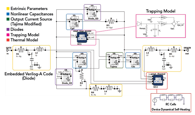
Figure 1 GaN HEMT transistor model from a pre-release AMCAD compact modeling tool.
It is important to mention that the nonlinearities are modeled using Verilog-A code. This standard is widely used in many EDA tools, allowing easy transfer between different software platforms. With compact modeling extraction, it becomes necessary to perform various measurement types to extract the different model parameters.
CHARACTERIZING GAN HEMT TRANSISTORS FOR RF APPLICATIONS
The I-V characteristic is essential for estimating the performance of RF power transistors.2 The characterization is carried out in a pulse-mode measurement to overcome self-heating. The pulsed I-V system is combined with a vector network analyzer (VNA) to obtain the scattering parameters for each pulsed bias point. Using this technique, it is possible to extract linear models from all the I-V characteristics and to derive the nonlinear model.
Thermal effects are key aspects of RF power transistors.3 These effects are especially important when working with modulated signals that may have short- and long-term memory effects. Electrical methodologies have been developed to measure these thermal effects. These techniques are based on pulsed and/or DC I-V measurements done at different chuck temperatures. The aim is to characterize a given parameter, like on-resistance, gate or drain currents, as a function of the dissipated power and the chuck temperature.
The trap phenomenon is another important aspect to consider for GaN HEMT transistors. Traps have a significant impact on the achievable performance of GaN technology. These traps result from impurities or defects in the crystal lattice or on its surface. A pulsed-mode measurement technique enables the characterization of the transient effects induced by traps in the component while avoiding thermal effects.
COMPACT MODEL EXTRACTION AND SIMULATION OF A GAN HEMT TRANSISTOR
The process of extracting a compact model is sequential and incremental. The process involves CAD software that may embed DC, AC, transient, harmonic balance and other different kinds of simulation engines. Using these tools, it is possible to compute the circuit response of the model in conditions close to those used in the actual characterization measurement.
The model extraction process starts with determining the linear and the nonlinear model elements.4 These elements include the diodes, the output current source and the nonlinear capacitors. Then, thermal and trap models are added.5 Thanks to transient simulations, the model response over pulsed stimuli can be obtained.
Finally, the model is compared against large-signal measurements obtained using a VNA-based load-pull system. Harmonic balance analysis is used to compute the periodic steady-state response to get the AM-AM and AM-PM characteristics for different load impedances and conditions close to the final application. Figure 2a shows a comparison between modeled and measured large-signal performance and contours at load impedances that result in 3 dB gain compression from the maximum output power. Figure 2b shows the same modeled and measured large-signal performance and contours at load impedances that result in maximum power-added efficiency at 3 dB compression. The measurements were performed at 3.6 GHz on a GaN-on-SiC HEMT device with four gate fingers and a 220 µm gate width. The contours show good agreement between the measured results and the model. The graphs showing output power (Pout), PAE, gain (Gp) and output current (Iout) are plotted as a function of delivered input power (Pin) for the specific load impedance.
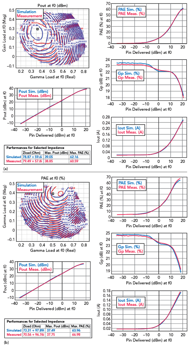
Figure 2 (a) Large-signal performance at 3 dB gain compression. (b) Power-added efficiency performance at 3 dB gain compression.
These results are an invaluable source of information for the model engineer and the design engineer. From these results, the model may be adjusted to better match the actual results. Thanks to the versatility of the Verilog-A format, the model can be transferred to the design engineer at this step to complete the RF PA design.
TRANSISTOR-LEVEL TO SYSTEM-LEVEL SIMULATION
Recent advancements in EDA software have revolutionized the design of increasingly complex circuits. This has both enabled and accommodated the demands of increasingly sophisticated modern telecommunications technology. As an example, the adoption of advanced topologies like Doherty amplifiers boosts efficiency but further complicates design challenges. These tools now enable designers to meticulously simulate and optimize the performance of each component well before actual production begins. The aim is to harness all this preparatory work to enable comprehensive system-level evaluations that ensure that all components function harmoniously within the intended system architecture.
Behavioral models are essential throughout the design cycle of RF systems. Initially, these models facilitate the specification of system elements by creating a digital twin that guides the selection of suitable off-the-shelf components. As the design cycle progresses, these models become invaluable tools for developers of signal processing algorithms, digital predistortion techniques and control systems. These tools allow developers to test their solutions against realistic and comprehensive circuit impairment scenarios. This testing helps to ensure the effectiveness and robustness of the system. Finally, before system assembly, the digital twin is updated with the newly designed circuits, enabling a preliminary validation phase that incorporates measurements from various prototypes.
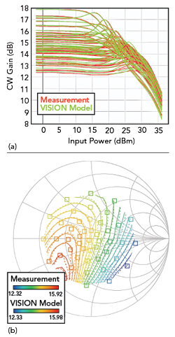
Figure 3 (a) CW gain at 2.65 GHz. (b) CW gain contours at Pin = 23 dBm.
As an example of the utility of this approach, high peak-to-average power ratios (PAPR) in modern communication signals induce strong amplitude fluctuations. These amplitude fluctuations can lead to signal distortions when amplified by nonlinear devices like PAs. Behavioral modeling presents a scalable solution by allowing the characterization of the nonlinearity, memory effects and dynamic responses of a PA to varying signal conditions without the extensive overhead of physical prototyping.
PA BEHAVIORAL MODEL EXTRACTION AND SIMULATION
Starting from circuit designs in EDA tools, PAs can be modeled at the transistor level to ensure that every nuance of electronic interaction is captured. These designs are typically simulated under various conditions that may include sweeping the power and carrier frequency of the CW input signal and PA load impedance to generate comprehensive data sets that better describe the behavior of the amplifier. Figure 3a shows the measured versus modeled responses of the load-pull gain characteristics of a 2.65 GHz PA with parameterized load impedance. Figure 3b shows measured versus modeled agreement for the gain contours of that same amplifier at Pin = 23 dBm. The excellent agreement shown in both figures is, in part, due to the behavioral model that faithfully reproduces the nonlinear characteristics of this PA designed for telecom base stations. In addition to the nonlinear characteristics, the model also takes into account the mismatch that can be introduced in active antenna architectures.
These data form the foundation for behavioral model extraction, which abstracts the response of the PA into an object that can be used for system-level simulations. The extraction of behavioral models necessitates a thorough analysis of the PA, particularly to describe its response to modulated signals. These signals often exhibit variable envelopes that are affected by low frequency memory effects. Techniques like two-tone tests are instrumental in identifying the nonlinearity and memory effects that manifest over a range of frequencies and power levels.
In scientific literature, behavioral models like the Volterra series and its truncated variants such as the Generalized Memory Polynomial (GMP) effectively capture the dynamics of a given signal and provide a suitable framework for use in PA linearization applications.6,7 This requires extracting the model, whenever necessary, following variations in signal characteristics. For system simulation, another approach that is like the method used in transistor modeling is applied. This method consists of extracting the coefficients in one pass, characterizing the high frequency and low frequency memory effects separately. This is formally known as the Two-Path Memory (TPM) model or High-Power Amplifier Unilateral with High Frequency and Low Frequency Memory Effects (HPA-U-HFLF) model.8 This method improves the robustness of the prediction by considering the various signal characteristics to which it will be exposed. This includes varying PAPR levels, from small-signal linear regimes to significant gain compression and a wide range of signal bandwidths from kHz to several GHz.
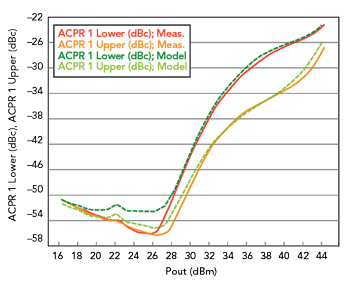
Figure 4 Measured and modeled ACPR simulation.
Figure 4 shows the measured and modeled ACPR results for the lower and upper channels of a PA stimulated by a 16-QAM signal, characterized by 4 dB PAPR and a bandwidth of 50 MHz. The results show an asymmetry highlighting the low frequency memory effects in the PA. They also show the ability of the behavioral model to predict these figures of merit over a wide average power range.
Recent work has made it possible to take into account nonlinearities, along with high and low frequency memory effects and mismatching in a single model. This enhanced TPM model, or the High-Power Amplifier Bilateral with High Frequency and Low Frequency Memory Effects (HPA-B-HFLF) model,9 was first tested on a PA circuit designed in PathWave ADS software provided by Keysight Technologies. The model was extracted using harmonic balance simulations (load-pull and two-tone analysis) and validated in an envelope transient simulation using a 1024-QAM signal with a 160 MHz bandwidth. The signal, with a PAPR of 6.6 dB, is substantial enough to markedly stimulate the nonlinear response characteristics of the PA. Figure 5a shows the lower ACPR contours and Figure 5b shows the upper ACPR contours. Figure 6 shows the EVM contours. These three plots use simulation results from the HPA-B-HFLF model, measured with an average input power of 10 dBm. This new behavioral model was tested with different load impedances and demonstrated an exceptional ability to predict spectral responses and key metrics, such as the ACPR results shown in Figure 5 and the EVM results shown in Figure 6 over a wide range of load impedances.
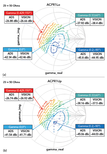
Figure 5 (a) Lower ACPR simulation results. (b) Upper ACPR simulation results.
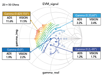
Figure 6 EVM contours.
In addition to the performance evidenced by the HPA-B-HFLF model, simulation times were deemed to be reasonable. This was particularly true when compared to the circuit-level simulation. For example, obtaining the ACPR and EVM contours took less than 10 minutes to simulate using the HPA-B-HFLF model. This is compared with one hour for a nominal simulation using the circuit design alone. This aspect of simulation time is one of the main reasons for using behavioral models.
CONCLUSION
The journey from GaN HEMT transistor characterization to the implementation of these devices in real-world systems underscores a significant advancement in telecommunications technology. This progression illustrates the crucial role of advanced modeling and simulation techniques in bridging the gap between microscopic electronic behavior and macroscopic system performance. By leveraging sophisticated compact modeling, engineers can predict and optimize the performance of PAs more accurately, leading to more efficient and robust telecommunication systems. Furthermore, the integration of behavioral models into the system-level evaluations not only enhances design accuracy but also reduces development time and costs, enabling faster market deployment. This comprehensive approach, from transistor-level analysis to the system-level application, is crucial for meeting the burgeoning demands of next-generation wireless technologies, ensuring that new telecommunications infrastructure is both powerful and reliable.
References
- C. Charbonniaud, A. Xiong, S. Dellier, O. Jardel and R. Quéré, “A Nonlinear Power HEMT Model Operating in Multi-bias Conditions,” 2010 European Microwave Integrated Circuits Conference Digest (EuMIC), pp. 34-137.
- J. P. Teyssier, P. Bouysse, Z. Ouarch, D. Barataud, T. Peyretaillade and R. Quere, “40 GHz/150 ns Versatile Pulsed Measurement System for Microwave Transistor Isothermal Characterization,” IEEE Transactions on Microwave Theory and Techniques, Vol. 46, No. 12, December 1998, pp. 2043-2052.
- J. A. Lonac, A. Santarelli, I. Melczarsky and F. Filicori, “A Simple Technique for Measuring the Thermal Impedance and the Thermal Resistance of HBTs,” 2005 European Gallium Arsenide and Other Semiconductor Application Symposium Digest, EGAAS, pp. 197-200.
- G. Dambrine, A. Cappy, F. Heliodore and E. Playez, “A New Method for Determining the FET Small-Signal Equivalent Circuit,” IEEE Transactions on Microwave Theory and Techniques, Vol. 36, No. 7, July 1988, pp. 1151-1159.
- O. Jardel, F. De Groote, T. Reveyrand, C. Charbonniaud, J.P. Teyssier, D. Floriot and R. Quéré, “An Electrothermal Model for AlGaN/GaN Power HEMTs Including Trapping Effects to Improve Large-Signal Simulation Results on High VSWR,” IEEE Transactions on Microwave Theory and Techniques, Vol. 55, No. 12, December 2007, pp. 2660-2669.
- J. C. Pedro and S. A. Maas, “A Comparative Overview of Microwave and Wireless Power-Amplifier Behavioral Modeling Approaches”, IEEE Transactions on Microwave Theory & Techniques, Vol. 53, No. 4, pp. 1150-1163, April 2005.
- D. Schreurs and al., RF Power Amplifier Behavioral Modeling, Cambridge, U.K: Cambridge Univ. Press, 2008.
- E. Ngoya and S. Mons, “Progress for Behavioral Challenges”, IEEE Microwave Magazine, Vol. 15, No. 6, pp. 91-105, September 2014.
- W. Saabe, C. Mazière, A. Delias, S. Mons, E. Ngoya, “RF Power Amplifier Model Extraction for Accurate and Fast Load Pull Simulations with Wideband Signals,” 103rd ARFTG Microwave Measurement Conference (ARFTG), Washington DC, USA, 2024.