

A 71.5 to 81 GHz 6-bit phase shifter in 40 nm CMOS incorporates a compact differential capacitor-free quadrature generator circuit (QGC) based on a folded transformer for I/Q generation and size reduction. A transformer-based series peaking technique is also used for bandwidth extension. The phase shifter demonstrates a 3 dB bandwidth from 71.5 to 81 GHz. Its RMS phase error is 3.2 to 3.6 degrees and its RMS gain error is 0.85 to 0.90 dB. The phase shifter’s core area is 250 × 720 μm.
To improve signal-to-noise ratio and reduce interference, beamforming techniques based on phased array systems have been widely applied in mmWave communication.1,2 In phased array systems, the phase shifter is a key component. Its phase resolution and phase shifting range determine the array system’s beamforming and beam steering capabilities.3,4 Phase shifters can generally be classified as passive5,6 and active.7,8 Switched,9 reflection10 and load transmission line phase shifters are all passive. They generally occupy large physical areas and have high insertion loss, while active phase shifters offer better phase resolution, lower insertion loss and smaller size.
A conventional active phase shifter typically contains several inductors and this consumes a large area.11 In addition, the performance of the variable gain amplifier (VGA) limits the phase resolution. There are typically two methods to implement the VGA: tail current-controlled Gilbert cell11 and current steering.12 Regardless of the approach, phase resolution is poor because the VGA is difficult to adjust. At mmWave frequencies, this is more pronounced due to limited transistor performance and parasitic effects in CMOS design.
To address these issues, this article presents a 6-bit active phase shifter employing a compact QGC and a proportional digital-to-analog converter (DAC) array with a 6-bit decoder. It demonstrates an RMS phase error of 3.2 to 3.6 degrees and an RMS gain error of 0.85 to 0.90 dB from 71.5 to 81 GHz. This performance is achieved without digital calibration.
PHASE SHIFTER DESIGN
The phase shifter comprises a compact capacitor-free QGC, a three-stage amplifier and an I/Q DAC array for phase synthesis with a 6-bit decoder. Input and output baluns are added to enable measurements. After two stages of amplification, fully differential I/Q signals are created by the QGC. Interstage matching in the I/Q path between the QGC and the amplifier is employed for maximum power transmission. The binary-weighted I/Q DAC and 6-bit decoder are co-designed for vector synthesis. Series peaking between the amplifier and DAC is used for bandwidth extension. The phase shifter block diagram is shown in Figure 1.
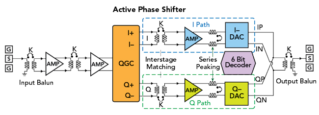
Figure 1 Active phase shifter block diagram.
QGC Design
The QGC plays a critical role because it generates the orthogonal I/Q signals and directly affects phase shifter performance. Many traditional transformer-based QGCs employ a planar structure with horizontal coupling, but this wastes area. To solve this problem, the design described by Li et al.13 is a vertically stacked structure with vertical coupling. However, this approach increases design complexity due to considerations regarding capacitor design and placement when adding additional capacitors.
In the phase shifter design described in this article, parasitic capacitors are used between metal layers. The equivalent circuit and layout of the QGC are shown in Figure 2a and Figure 2b, respectively. A differential input signal is applied to the input ports (IN+, IN-) and then split into two quadrature signals at the through (THU+, THU-) and coupled (CPL+, CPL-) ports.14 A 100 Ω resistor is connected between two isolation ports (ISO+, ISO-). Cp is the parasitic capacitance at different physical layers. In 40 nm CMOS technology, the thickness of the upper layer metal is thicker and its resistivity is lower. This is beneficial for reducing insertion losses. Therefore, the top four metal layers are used for the QGC layout.
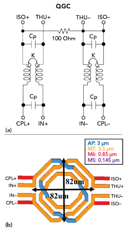
Figure 2 (a) QGC schematic. (b) QGC layout.
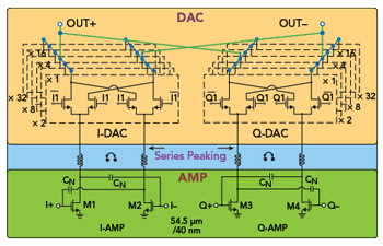
Figure 3 Schematic of the amplifier, series peaking and I/Q DAC.
Amplifier and I/Q DAC Design
The amplifier and DAC schematic in the I/Q path is shown in Figure 3. In the amplifier section, a capacitor, CN, neutralizes the gate-to-drain capacitance. Series peaking is used between the amplifier and DAC for bandwidth extension. In the DAC section, all transistors are controlled by a 6-bit decoder. To achieve phase accuracy, transistor size ratios in the DAC are optimized to be 1:2:4:8:16:32.
Series Peaking Technique
Parasitic capacitance from the amplifiers and DACs narrows the phase shifter bandwidth. There are at least two techniques to mitigate this: series peaking and parallel peaking. These techniques apply the principles of LC series resonance and LC parallel resonance, respectively. The inductance for both series and parallel resonance is shown in Equation 1:

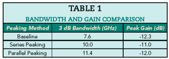
Simulation results for the phase shifter, along with the peaking results are plotted in Figure 4 and listed in Table 1. The results show the improvement in bandwidth and peak gain using the two peaking methods. The baseline is with no resonant inductor. Both series peaking and parallel peaking improve the 3 dB bandwidth. Without the resonant inductor, the 3 dB bandwidth is 7.6 GHz. With series and parallel peaking, the bandwidth is 10 GHz and 11.4 GHz, respectively. Although the bandwidth is slightly reduced, series peaking is chosen for this design due to its higher peak gain.
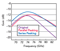
Figure 4 Simulated phase shifter bandwidth and peak gain.
The layout of the added series peaking inductor is shown in Figure 5. The inductor is rotationally arranged to reduce size. Therefore, transformer-based series peaking is adopted to improve bandwidth and gain and also to reduce chip size.
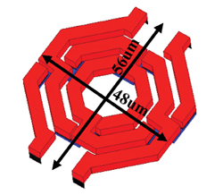
Figure 5 Transformer-based series peaking inductor layout.
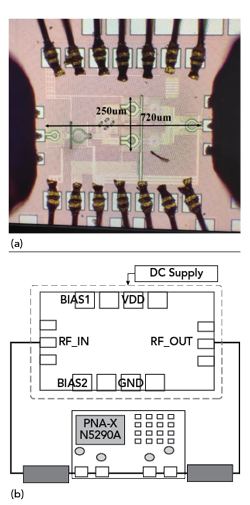
Figure 6 (a) 6-bit phase shifter die. (b) Measurement setup block diagram.
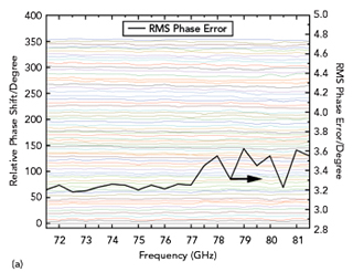
Figure 7a Relative phase shift performance.
Figure 7b Insertion loss performance.
MEASUREMENTS
The phase shifter chip shown in Figure 6a is implemented in 40 nm CMOS technology with a core area of 250 × 720 μm2. Figure 6b is the measurement setup block diagram. Measurements reveal a 3 dB bandwidth of 71.5 to 81 GHz and an insertion loss of 6 to 9 dB for one basic stage. The entire phase shift range is 360 degrees with a minimum phase resolution of 5.625 degrees. Figure 7a is the measured relative phase shift and Figure 7b is the insertion loss of the 64 states. The RMS phase error is below 3.6 degrees and the RMS gain error is less than 0.9 dB from 71.5 to 81 GHz. Performance characteristics and comparisons with other work are summarized in Table 2. The derivation of the FoM in Table 2 is shown in Equation 2:
(2)

CONCLUSION
A wideband 6-bit active phase shifter with three-stage amplification employs a compact and capacitor-free QGC with series peaking for quadrature signal generation and bandwidth extension. The phase shifter chip is implemented using TSMC’s 40 nm CMOS with a core area of 250 × 720 μm. A peak gain of -6 dB at 76.5 GHz and a 3 dB bandwidth from 71.5 to 81 GHz are achieved. Within the 3 dB bandwidth, the RMS phase error is 3.2 to 3.6 degrees and the RMS gain error is 0.85 to 0.90 dB. Its compact size and low phase error make this phase shifter suitable for application in mmWave phased array systems.
References
- T. Sowlati, S. Sarkar, B. Perumana, W. L. Chan, B. Afshar, M. Boers, D. Shin, T. Mercer, W. -H. Chen, A. P. Toda, A. G. Besoli, S. Yoon, S. Kyriazidou, P. Yang, V. Aggarwal, N. Vakilian, D. Rozenblit, M. Kahrizi, J. Zhang, A. Wang, P. Sen, D. Murphy, M. Mikhemar, A. Sajjadi, A. Mehrabani, B. Ibrahim, B. Pan, K. Juan, S. Xu, C. Guan, G. Geshvindman, K. Low, N. Kocaman, H. Eberhart, K. Kimura, I. Elgorriaga, V. Roussel, H. Xie, L. Shi and V. Kodavati, “A 60 GHz 144-Element Phased-Array Transceiver with 51 dBm Maximum EIRP and ± 60 Degree Beam Steering for Backhaul Application,” IEEE International Solid-State Circuits Conference, February 2018.
- K. Kibaroglu, M. Sayginer and G. M. Rebeiz, “A Low-Cost Scalable 32- Element 28-GHz Phased Array Transceiver for 5G Communication Links Based on a 2×2 Beamformer Flip-Chip Unit Cell,” IEEE Journal of Solid-State Circuits, Vol. 53, No. 5, May 2018, pp. 1260–1274.
- B. Sadhu, Y. Tousi, J. Hallin, S. Sahl, S. K. Reynolds, Ö. Renström, K. Sjögren, O. Haapalahti, N. Mazor, B. Bokinge, G.Weibull, H. Bengtsson, A. Carlinger, E. Westessen, J. E. Thillberg, L. Rexberg, M. Yeck, X. Gu, M. Ferriss, D. Liu, D. Friedman and A. Valdes-Garcia, “A 28-GHz 32-Element TRX Phased-Array IC with Concurrent Dual-Polarized Operation and Orthogonal Phase and Gain Control for 5G Communications,” IEEE Journal of Solid-State Circuits, Vol. 52, No. 12, December 2017, pp. 3373–3391.
- W. Zhu, W. Lv, B. Liao, Y. Zhu, Y. Dai, P. Li, L. Zhang and Y. Wang, “A 21 to 30-GHz Merged Digital-Controlled High Resolution Phase Shifter-Programmable Gain Amplifier with Orthogonal Phase and Gain Control for 5-G Phase Array Application,” IEEE Radio Frequency Integrated Circuits Symposium, June 2019.
- K. T. Trinh, C. -H. Lin, H. -L. Kao, H. -C. Chiu and N. C. Karmakar, “18 - 20 GHz Compact Passive 4-Bit GaAs MMIC Phase Shifter with Low Insertion Loss,” IEEE Asia-Pacific Microwave Conference, December 2019.
- C. Chen, Y. Wang, Y. Lin, Y. Hsiao, Y. Wu and H. Wang, “A 36 - 40 GHz Full 360 Degree Ultra-Low Phase Error Passive Phase Shifter with a Novel Phase Compensation Technique,” European Radar Conference, October 2017.
- Z. Duan, Y. Wang, W. Lv, Y. Dai and F. Lin, “A 6-bit CMOS Active Phase Shifter for Ku-Band Phased Arrays,” IEEE Microwave and Wireless Components Letters, Vol. 28, No. 7, July 2018, pp. 615–617.
- B. Cetindogan, E. Ozeren, B. Ustundag, M. Kaynak and Y. Gurbuz, “A 6 Bit Vector-Sum Phase Shifter with a Decoder Based Control Circuit for X-Band Phased-Arrays,” IEEE Microwave and Wireless Components Letters, Vol. 26, No. 1, January 2016, pp. 64–66.
- D. Huang, L. Zhang, D. Li, L. Zhang, Y. Wang and Z. Yu, “A 60-GHz 360 Degree 5-Bit Phase Shifter with Constant IL Compensation Followed by a Normal Amplifier with 1 dB Gain Variation and 0.6-dBm OP-1dB,” IEEE Transactions on Circuits and Systems II: Express Briefs, Vol. 64, No. 12, December 2017, pp. 1437–1441.
- J. Xia, M. Farouk and S. Boumaiza, “Digitally-Assisted 27-33 GHz Reflection-Type Phase Shifter with Enhanced Accuracy and Low IL-Variation,” IEEE Radio Frequency Integrated Circuits Symposium, June 2019.
- X. Quan, X. Yi, C. C. Boon, K. Yang. C. Li, B. Liu, Z. Liang and Y. Zhuang, “A 52-57 GHz 6-Bit Phase Shifter with Hybrid of Passive and Active Structures,” IEEE Microwave and Wireless Components Letters, Vol. 28, No. 3, March 2018, pp. 236–238.
- B. Wang, H. Gao, M. K. Matters-Kammerer and P. G. M. Baltus, “A 60 GHz 360 Degree Phase Shifter with 2.7 Degree Phase Resolution and 1.4 Degree RMS Phase Error in a 40-nm CMOS Technology,” IEEE Radio Frequency Integrated Circuits Symposium, June 2018.
- Y. Li, Z. Duan, W. Lv, D. Pan, Z. Xie, Y. Dai and L. Sun, “A 32-40 GHz 7-bit CMOS Phase Shifter with 0.38 dB/1.6 Degree RMS Magnitude/Phase Errors for Phased Array Systems,” IEEE Radio Frequency Integrated Circuits Symposium, August 2020.
- S. Li, G. Feng, Y. Zou and Y. Wang, “A Compact 58-65 GHz 6-Bit Phase Shifter with 0.7 deg/0.35 dB RMS Phase/Gain Error in 40 nm CMOS Technology,” IEEE MTT-S International Wireless Symposium, August 2022.
- D. Pepe and D. Zito, “Two mmWave Vector Modulator Active Phase Shifters with Novel IQ Generator in 28 nm FDSOI CMOS,” IEEE Journal of Solid-State Circuits, Vol. 52, No. 2, February 2027, pp. 344–356.
- J. Jang, B. Kim, C. -Y. Kim and S. Hong, “79-GHz Digital Attenuator-Based Variable-Gain Vector-Sum Phase Shifter with High Linearity,” IEEE Microwave and Wireless Components Letters, Vol. 28, No. 8, August 2018, pp. 693–695.
- G. H. Park, C. W. Byeon and C. S. Park, “A 60-GHz Low-Power Active Phase Shifter with Impedance-Invariant Vector Modulation in 65-nm CMOS,” IEEE Transactions on Microwave Theory and Techniques, Vol. 68, No. 12, December 2020, pp. 5395–5407.
- E. -T. Sung, S. Wang and S. Hong, “A 60-GHz Polar Vector Modulator with Lookup Table-Based Calibration,” IEEE Microwave and Wireless Components Letters, Vol. 31, No. 6, June 2021, pp. 572–574.
- Z. Li, J. Qiao and Y. Zhuang, “An X-Band 5-Bit Active Phase Shifter Based on a Novel Vector-Sum Technique in 0.18 μm SiGe BiCMOS,” IEEE Transactions on Circuits and Systems II: Express Briefs, Vol. 68, No. 6, June 2021, pp. 1763–1767.
- K. Zhao, L. Qiu, J. Chen, Q. Dong, Y. -C. Kuan, Q. J. Gu, C. Song and Z. XU, “An E-Band Subradix Active Phase Shifter with < 0.69 Degrees RMS Phase Error and 16-dB Attenuation in 28-nm CMOS,” IEEE/MTT-S International Microwave Symposium, June 2022.
- M. Ghaedi Bardeh, J. Fu, N. Naseh, J. Paramesh and K. Entesari, “A Wideband Low RMS Phase/Gain Error mmWave Phase Shifter in 22-nm CMOS FDSOI,” IEEE Microwave and Wireless Technology Letters, Vol. 33, No. 6, June 2023, pp. 739–742.