

High gain and panel-mountable antennas are essential to enable future mmWave-based portable devices to establish a feasible cellular communication link. Conventional antenna design techniques might be inadequate to meet these design and physical footprint criteria. To address these challenges, metamaterials (MTMs) might provide a useful tool to improve the gain and other performance metrics of high gain antennas specifically designed for mmWave 5G portable devices. This article delves into the application of the sub-wavelength MTM structures for compact, high gain antennas. The end-fire gain enhancement technique is initially explored, followed by broadside gain enhancement. Case studies of the two antennas are also presented. Mutual coupling reduction techniques using electrically small MTM structures are also discussed.
With the explosion of data usage among smartphone users, researchers and pundits across the globe have been contemplating feasible solutions to accommodate this growth.1 As the number of users grows, so too does the bandwidth required by these users. To fulfill these technical requirements, the spectral efficiency of the current communication channels could be exploited. The critical problem with this approach is that the achievable upper limit of spectral efficiency is finite and communication theoreticians believe that the current protocols in place are already approaching this theoretical limit.
The primary challenge for the communication link at mmWave frequencies is the relatively high free space path loss compared to its microwave counterparts. Among the strategies to overcome this issue is to design and deploy numerous low-power base station towers. Even if the radiated powers of base station towers are increased within a given geographical radius, the received power at the mobile device would still be well below the receiver’s sensitivity. Thus, the only viable option for a successful implementation of the mmWave link is to integrate high gain antennas within the mobile terminal and base stations.2 This compromises the angular coverage, so alternate strategies to optimize coverage need to be explored for a real-world deployment. The design of high gain compact antennas in the context of portable devices is the theme of this article.
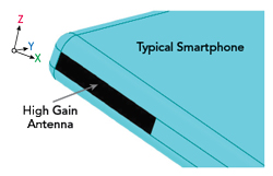
Figure 1 Typical layout of a commercial 5G portable device.
It must also be noted that the pre-existing infrastructure and industrial processes used to manufacture sub-6 GHz antennas could be tweaked to manufacture antennas operating in and around the 28 GHz band. A typical smartphone case is depicted in Figure 1 with the dimensions adopted from a successful, widely-used commercial smartphone model. The available footprint to integrate high gain antennas or antenna systems is very limited. A typical dimensional requirement would be 7 mm (panel height) × 10 mm (tentative width) × 3 mm (expected depth). If these dimensions are expressed electrically, it translates to 0.65 λ × 0.93 λ × 0.28 λ, with λ computed at 28 GHz. These values indicate that the electrical footprint for antenna integration is minimal. Hence, compact antennas with maximum gain for the available effective radiating aperture are necessary for 5G portable devices.
Numerous techniques have been reported in literature to enhance the gain of planar antennas. For instance, metal strip parasitics can be loaded in the radiating aperture for gain enhancement or a dielectric lens could be integrated with a broadside radiator for a narrower unidirectional beam. Both strategies deliver lower gain for the occupied radiating volume. The other popular strategy is to minimize the losses within the substrate to boost gain in the forward direction but the quantum of gain enhancement would be in the vicinity of 1 dB. A printed ridge gap waveguide method can also be used for dielectric loss reduction.3
Another strategy is to implement phased arrays within the smartphone panel.4 This strategy increases the complexity of the antenna system. Also, beam locking between the transmitter and receiver has to be programmed and dynamically updated. Thus, to implement high gain antennas with minimal electrical and physical footprint, MTM integration seems to be an optimal solution.
MTM are periodic sub-wavelength geometries. When they are integrated with an antenna, the performance metrics of the antenna will be altered.5 As these are primarily sub-wavelength geometries, the same could be explored for gain enhancement with an electrically small protrusion of the dielectric suitable for 5G portable devices.
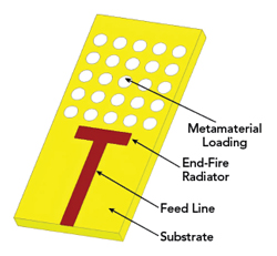
Figure 2 Generic layout of a typical end-fire metamaterial loading.
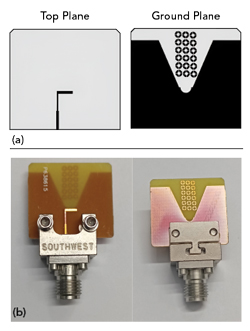
Figure 3 (a) Schematic of the proposed TSA integrated with ZIM. (b) Fabricated TSA integrated with ZIM prototype.
The rest of the article addresses the benefits of MTMs for a variety of applications. The end-fire or planar gain enhancement using MTM loading is discussed in the next section, followed by an explanation of the role of MTMs in the context of broadside radiators. This will be followed by a discussion of mutual coupling reduction in phased arrays with the application of periodic structures. Even though MTMs have been exhaustively illustrated for the miniaturization6 of microwave antennas, the same might not be relevant in the mmWave domain. The primary reason for this thesis is that the physical size of the mmWave antennas is typically less than 10 mm (or in the vicinity of 1 λ at 28 GHz), alleviating the requirement for further miniaturization to make antennas compatible with portable devices.
END-FIRE GAIN ENHANCEMENT
End-fire antennas radiate in the same plane as that of the antenna’s orientation. Two primary types of end-fire radiators are resonant, like printed dipole and printed Yagi-Uda antennas and traveling wave, like printed antipodal and Vivaldi antennas. End-fire antennas are important for portable 5G devices. The primary reason for this is that end-fire antennas radiate away from the user when integrated with portable devices. MTMs could be loaded onto an end-fire antenna for gain enhancement without significantly altering the physical footprint of the element. For these applications, MTM unit cells could yield high gain and be electrically compact.
A generic schematic of an end-fire antenna integrated with MTMs is shown in Figure 2. This architecture incorporates a PCB-based radiator fed by a microstrip line. The antenna is printed on an electrically-thin substrate to avoid surface wave modes.2 The radiating aperture must be placed at least a wavelength away from the feed plane to avoid pattern contamination due to the connector.4 This could be neglected in the commercial deployment of the antennas. The radiator could be either resonant or traveling wave type. Hence, the anticipated unidirectional pattern would be away from the radiator, traversing through the dielectric integrated with the sub-wavelength unit cells as shown. These unit cells aid in the phase correction of the E-fields emanating from the aperture, resulting in higher antenna gain. The length and width of the MTM spread would be electrically small, typically 0.5 to 1 λ, saving significant RF real estate. Most of the reported designs in the literature are based on the generic layout shown in Figure 2.
A tapered slot antenna (TSA) integrated with zero-index metamaterial (ZIM) unit cells is illustrated in Figure 3a. The unit cells aid in the phase correction of the electric field emanating from the microstrip to slot line transition. The proposed antenna is designed on a low-cost FR4 substrate with a thickness of 0.5 mm. Since the substrate is electrically thin, the dielectric losses encountered within the substrate are negligible even in Ka-Band. The gap within the ZIM was maintained at 100 μm, due to the limitation of the photolithography technique. The fabricated antenna is displayed in Figure 3b.
The simulated and measured input reflection coefficients are shown in Figure 4. The -10 dB bandwidth is from 26.45 to 28.94 GHz, translating to 9 percent. The narrow bandwidth is attributed to the electrical thickness of the substrate and the design of the transition from the standard 50 Ω feed line to the slot line.
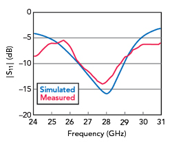
Figure 4 |S11| of the proposed TSA integrated with ZIM.
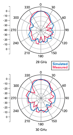
Figure 5 E-plane patterns of the proposed TSA integrated with ZIM.
The E-plane radiation patterns are illustrated in Figure 5. The front-to-back ratio is greater than 10 dB across the operational bandwidth. It must also be noted that the patterns have minimal variation across the bandwidth. The pattern integrity is high due to the layout of the ZIM unit cells in the radiating aperture of the proposed antenna.
The gain enhancement of the antenna is close to 1 dB across the entire spectrum, as evident from Figure 6. The quantum of gain enhancement is not high due to the number of unit cells available in the physical aperture of the proposed antenna. Gain enhancement up to 3 dB could be achieved with this technique by integrating unit cells in the H-plane.
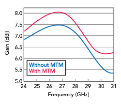
Figure 6 Forward on-axis gain of the proposed TSA integrated with ZIM.
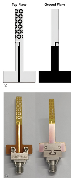
Figure 7 (a) Schematic of proposed printed dipole integrated with ZIM. (b) Fabricated TSA integrated with ZIM prototype.
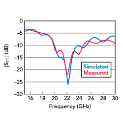
Figure 8 |S11| of the proposed printed dipole integrated with ZIM.
Another strategy involves integrating the ZIM unit cells with resonant structures such as a printed dipole, is illustrated in the circuit layouts of Figure 7a. The proposed antenna is designed on a low-cost FR4 substrate with a thickness of 0.5 mm. The ZIM unit cells integrated within the extended dielectric of the printed dipole help increase the antenna gain.
Conventional half-wavelength parasitics also yield a similar gain with a compromise in the real estate and the operating bandwidth. The proposed element is only 4.9 mm wide, which could be easily integrated with 5G smartphones that typically have a panel height of 8 mm. The fabricated prototype is shown in Figure 7b. The dimensions of the unit cells are maintained to be within the fabrication limits.
The simulated and measured input reflection coefficients are illustrated in Figure 8. The proposed antenna offers an impedance bandwidth of 5.3 GHz, translating to 23.7 percent. The wide bandwidth can be attributed to the impedance-matched feed structure and the wideband behavior of the ZIM unit cells. The bandwidth is relatively high even with the use of an electrically-thin substrate. The design could be scaled to any band by varying the dimensions of the dipole arms and the slot size within the ZIM unit cells.