

GaN electronic devices, especially GaN-based high electron mobility transistors (HEMTs), are increasingly used in RF and power conversion applications. Yet in the most demanding applications, GaN device performance and reliability may be limited by thermal considerations such as the channel temperature. Some forms of enriched monocrystalline synthetic diamond have been shown to have the highest thermal conductivity of any known solid at room temperature.1 Because of this thermal conductivity, the integration of diamond into GaN electronic structures can significantly improve the thermal management of GaN devices. However, such integration has been technically challenging so far. In its latest GaN electronics reports,2 KnowMade highlights endeavors to leverage GaN with diamond integration in electronic devices based on the recent patent applications filed in this space.
MANY IP NEWCOMERS ENTER THE FIELD
The patent analysis is broad. It considers all patent applications claiming the integration of diamond with GaN electronics without distinction of the material, so it includes applications using single-crystal diamond, polycrystalline diamond and other varieties. The analysis does not differentiate as to the stage of the process where the diamond was integrated. This integration can be a passivation layer, a substrate, a heat sink or another use. It also does not distinguish whether the diamond was integrated as epitaxy, bonding or in some other fashion.
With these guidelines, Figure 1 describes the time evolution of intellectual property (IP) activities related to the technical challenge of integrating diamond materials with GaN. As Figure 1 shows, patenting activities were very limited in the 2000s, but they took off in the early 2010s. The driving forces behind the increase in patent activity were the efforts of pioneers such as Element Six and Group4 Labs.
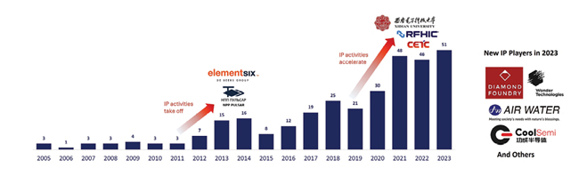
Figure 1 Number of inventions (patent families) related to diamond materials with GaN electronics. Source: KnowMade.
Founded in 2003 as a U.S. startup company, Group4 partnered with Element Six in 2008. Group4 was subsequently acquired by Element Six in 2013. In 2016, newly established Akash Systems agreed with RFHIC to jointly negotiate the repurchase of Element Six’s GaN-on-diamond IP. Akash acquired all patents and other IP rights related to GaN-on-diamond technology for use in satellite communications and related markets.
In 2021, the number of patent filings increased sharply, mainly due to the acceleration of Chinese players such as CETC with 29 inventions and Xidian University with 44 inventions. Since 2021, a relatively stable patenting activity has been observed, supported by the entrance of more than 30 new IP players, especially Chinese research organizations like Wuhan University, Shenzhen University and Taiyuan University of Technology, along with Chinese industrial players like CoolSemi, CSMH and others.
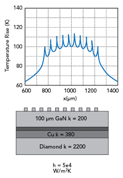
Figure 2 Diamond Foundry patent drawing for a single-crystal diamond wafer.
Besides China, several players like Air Water in Japan, which collaborated with Osaka Metropolitan University, have entered the field recently. This collaboration co-filed patent WO2023/048160, published in early 2023. The patent publication was followed by a scientific paper released in late 2023.3 In this paper, researchers described a method based on the heteroepitaxy of GaN on a 3C-SiC layer formed on a silicon substrate. Then, the silicon substrate is removed and the GaN-on-3C-SiC stack is bonded to a thermally conductive support layer that can be made of either diamond or polySiC, according to the first patent claim. So far, about 30 patent families have disclosed methods based on bonding techniques to integrate diamond materials with GaN electronic devices.
However, the bonding of GaN materials with a diamond substrate is technically challenging and alternative methods have been developed. For instance, Wonder CVD, a startup company founded in 2016 and headquartered in Dubai, entered the GaN electronics patent landscape in 2023, filing patent application US20230307249. It describes the growth of polydiamond on the silicon (111) thin layer of an SOI substrate, the removal of the base and oxide layers, followed by the heteroepitaxy of GaN on the other surface of the silicon (111) thin layer.
Another interesting example is the collaboration between imec and UHasselt in Europe that is described in patent EP4125113, although the patent application seems to have been abandoned since August 2023. The invention relates to the formation of a nanocrystalline diamond layer that forms a stable connection between a GaN material and a polydiamond material. In addition, the nanocrystalline diamond layer is expected to further facilitate heat dissipation for GaN electronic devices.
While the previous examples describe the integration of diamond materials in contact with or relatively close to the GaN device layer, U.S. startup company Diamond Foundry entered the GaN electronics patent landscape in 2023 with a different approach. In patent application US20230411459, Diamond Foundry disclosed a diamond substrate that could be used as a packaging substrate for GaN or SiC devices intended as an alternative to silicon-based IGBT chips used in electric vehicle applications. Diamond Foundry is one of the few companies in this space targeting power applications. Overall, less than 10 percent of all inventions related to diamond integration explicitly target power electronics. Figure 2 shows a drawing from US20230411459 illustrating Diamond Foundry’s idea for their diamond substrate.
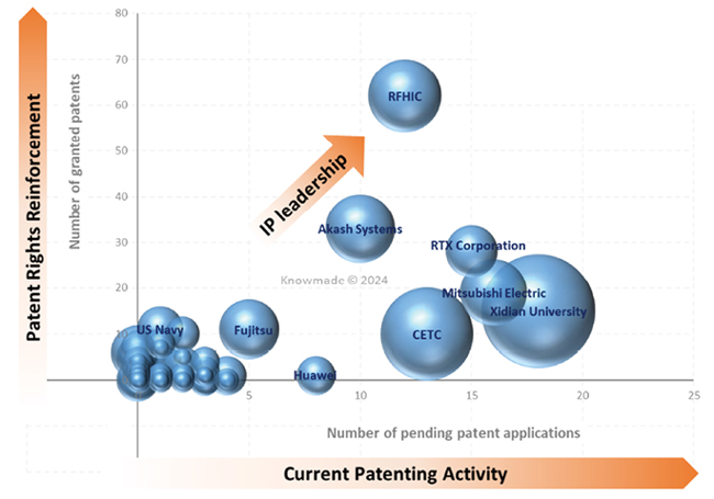
Figure 3 Integrating diamond into GaN IP leadership. Source: KnowMade.
THE IP LEADERS
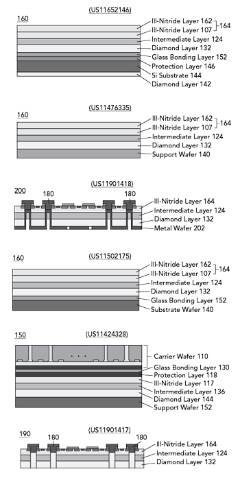
Figure 4 U.S. patents related to GaN/diamond wafers recently granted to RFHIC.
Comparing the number of pending patent applications with the number of granted patents for the main patent assignees provides valuable insight into the global IP competition for a given technology. Figure 3 shows this comparison for the integration of diamond materials with GaN electronics. Figure 3 plots the number of pending patent applications on the x-axis and the number of granted patents on the y-axis. At this intersection of these metrics, the size of the bubble represents the number of patent families selected for the study. The results of Figure 3 show that RFHIC stands as the current leader in GaN and diamond-related IP, but several RF GaN market players have positioned themselves as challengers. As can be seen, Akash Systems is the closest competitor to RFHIC, trailing slightly in patent applications and patents granted. However, companies like RTX Corporation, Mitsubishi Electric, Xidian University and CETC could pose strong future competition as all of them have more patent applications than RFHIC. Additionally, Mitsubishi Electric, Xidian University and CETC have comparable or much more breadth of GaN and diamond-related patent families. RFHIC’s current IP leadership is largely inherited from the patenting activities of Group4 and Element Six, although a few inventions were disclosed by RFHIC soon after the patent transaction in 2018.
In its 2023 GaN electronics IP report,4 KnowMade analyzed this IP leadership and pointed out RFHIC’s IP strength in GaN-on-diamond wafers and epiwafers, which is the very upward part of the RF GaN supply chain. In this part of the supply chain, RFHIC has no serious IP challengers but Xidian University. Because most of its patents are recent and exclusively filed in China, Xidian University’s IP leadership remains limited despite a relatively high number of inventions disclosed by the Chinese university. In contrast, RFHIC’s patent portfolio protects inventions in many different countries, especially in Europe, Japan, the U.S. and South Korea.
Interestingly, RFHIC resumed its patenting activities in 2021 with the publication of seven new inventions related to GaN-on-diamond. At the same time, they confirmed a global IP strategy, especially for one invention protected by several foreign patents, including six U.S. patents. The invention relates to the transfer of a III-nitride layer from its silicon growth substrate to a support wafer via a diamond layer. Different aspects of the method have been protected through various patent applications. For instance, an intermediate layer between the III-nitride layer and the diamond layer (US11652146), a composite silicon/diamond support wafer (US11652146) and the deposition of the support wafer (e.g., with polyGaN or polysilicon in US11476335), the carrier wafer (e.g., a SiC carrier is mentioned in US11424328) and the formation of through holes in such engineered substrates, as described in patent applications US11901418 and US11901417. Drawings from these and other patents granted to RFHIC for GaN/diamond wafers are shown in Figure 4.
Just like RFHIC, U.S. company Akash Systems published only a few inventions after the patent acquisition from Element Six. Akash published two patent families in 2018, mentioning the integration of diamond at the device level as a substrate and package level as a base for improved thermal management in transmitters used in satellite communication (US10332820, US10374553). Interestingly, the U.S. startup company resumed its IP activities in 2020, publishing seven inventions aiming to increase its coverage of the RF GaN supply chain. These recent inventions relate not only to packages, modules and systems but also to wafers, epiwafers and devices.
Mitsubishi Electric started its patenting efforts in 2017 and has maintained stable IP activity in the field. In contrast with other competitors aiming to protect inventions across the entire supply chain, Mitsubishi Electric’s IP strategy seems to focus on developing various aspects related to GaN-on-diamond device technology. Starting from an epiwafer, GaN layer transfer (US20230083507) and GaN bonding (US20220230920) techniques have been disclosed to integrate GaN devices with a diamond substrate. In an alternative approach, diamond may be integrated locally below the GaN devices with good adhesion characteristics and limited damage to the GaN epilayer. This concept is shown in Figure 5 with a drawing from US10720374 granted to Mitsubishi Electric in 2020. Additionally, the company has several patents related to the fabrication of GaN devices on recessed diamond substrates (e.g., US11482464).
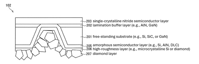
Figure 5 Formation of a diamond layer on a nitride layer.
CONCLUSION
IP activities related to the integration of diamond materials into GaN electronics devices have remained marginal in the GaN electronics patent landscape. For comparison, these activities represent less than 10 percent of all inventions related to RF GaN disclosed in 2023. Yet the analysis of the IP competition highlights a significant activity in recent years from several market players, in terms of the number of inventions disclosed by these players and the volume of patent applications filed to protect some of their key inventions in multiple countries. Additionally, since there is a limited number of well-established players in this space, there seems to be an opportunity for newcomers to make a breakthrough in this landscape, not only in terms of technology but also in terms of IP.
References
- “Material Properties of Diamond,” Wikipedia, Web: en.wikipedia.org/wiki/Material_properties_of_diamond#Thermal_conductivity.
- “All about GaN,” KnowMade, Web: knowmade.com/patent-analysis-expertise/semiconductor-expertise/power-electronics-devices-expertise/all-about-gan.
- R. Kagawa, Z. Cheng, K. Kawamura, Y. Ohno, C. Moriyama, Y. Sakaida, S. Ouchi, H. Uratani, K. Inoue, Y. Nagai, N. Shigekawa and J. Liang, “High Thermal Stability and Low Thermal Resistance of Large Area GaN/3C-SiC/Diamond Junctions for Practical Device Processes,” Wiley Online Library, Web: onlinelibrary.wiley.com/doi/10.1002/smll.202305574.
- “GaN Electronics Patent Landscape Analysis 2023,” KnowMade, November 2023, Web: nowmade.com/patent-analytics-services/patent-report/gan-electronics-patent-landscape-analysis-2023.