

5G terrestrial and satellite communications have already begun to use bands in frequency range 2 (FR2), with these frequencies ranging from 28 to 32 GHz. The signal propagation characteristics and short signal wavelengths in these high frequency bands limit the range of wireless communications. RF transceivers operating in these bands often rely on the integration of MIMO antenna systems to meet the link budget requirements and mitigate interference. For the ASIC designer, this means more channels, more radios and more digital signal processing.
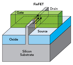
Figure 1 FinFET construction. Source: Synopsis.
Fin field-effect transistor (FinFET) device technology is becoming important for large MIMO systems. This transistor technology provides a high degree of flexibility while enabling digital radio solutions that can be based on RF analog-to-digital converters (ADCs) and digital-to-analog converters (DACs) that support multiple standards. Figure 1 shows a typical FinFET architecture.
FinFET construction results in a non-planar, 3D FET device. It gets the name “FinFET” because the source/drain region on the silicon surface resembles a fin. In this architecture, the gate structure is placed on the sides or wrapped around the fin. The advantage of this architecture is that the gate wraps around the vertical channel and conduction occurs on three sides as opposed to traditional planar structures where conduction occurs only at the surface of the channel. The increased surface area between the gate and channel provides better control and reduces leakage compared to planar FETs. Using the FinFET architecture results in better electrical characteristics than planar FETs, like faster switching times and higher current densities.
Despite the advantages, there are drawbacks to devices that implement this architecture. One of the more important drawbacks is power consumption. Figure 2 plots the energy/conversion-step figure of merit for high-resolution ADCs published in the last decade. It shows that the energy-per-conversion increases exponentially when operating above 1 GHz. As an example, increasing the sampling frequency from 1 to 5 GHz increases the converter power by more than 20×.
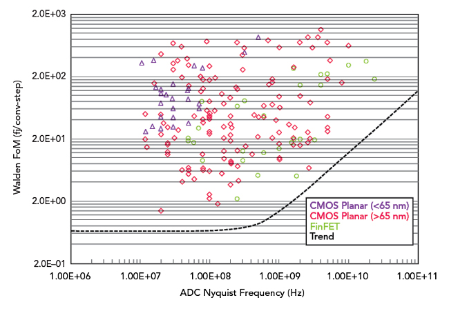
Figure 2 Walden fJ/conversion-step FoM as a function of the ADC frequency.
Significant power can be saved by designing an RF analog front-end. The benefit of this technique is that it allows the multi-GHz RF signal to be down-converted to a lower intermediate frequency (IF) signal, typically below 500 MHz. The transition to the digital domain is from these lower IF frequencies and this relaxes the constraints on the sampling frequency of the data converters.
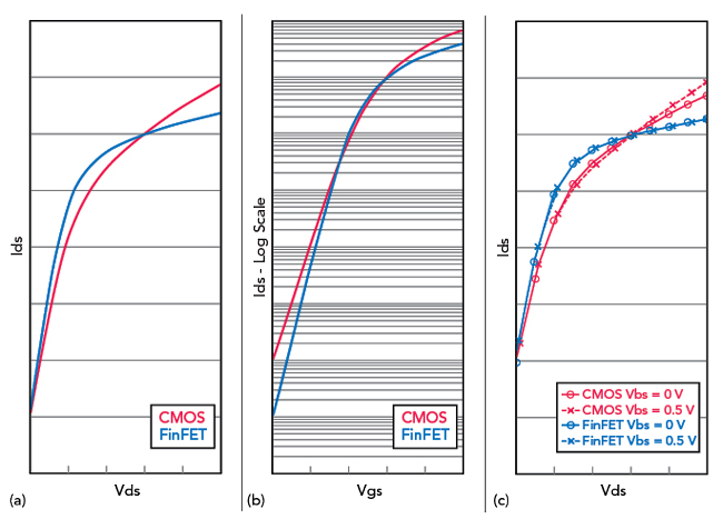
Figure 3 (a) Rout performance. (b) Threshold current performance. (c) Body bias performance.
Using FinFET architectures for analog design introduces other benefits. The architecture enables compact devices, and it has a high Gm and Rout. The subthreshold slope of the device is practically ideal, characterized by lower leakage and the high frequency performance is excellent, with peak fT values of 600 GHz. The PMOS versus NMOS β ratio is near a value of one and the threshold of the transistor is nearly unaffected by the body bias. Figure 3a shows a comparison of Rout performance for a FinFET device and a 40 nm planar CMOS device. Figure 3b shows subthreshold current comparisons for the same two devices and Figure 3c shows the body bias effect for the FinFET and CMOS devices.
Another drawback to this approach is manufacturing cost and complexity. This architecture requires 2x to 3x as many masks as planar devices require. This makes the analog layout complicated and slow, due to the large number of design rules and process steps. This also makes the technology better suited for digital place and route techniques. These drawbacks complicate the analog layout flow, especially when application performance demands 7 nm, or smaller, topologies. So, what can be done to minimize these challenges?
Here are some guidelines to make the process of designing analog FinFET ICs easier.
DO NOT MIX DEVICES THAT HAVE DIFFERENT DIMENSIONS
To make the chip modular, the analog designers should agree to a limited set of transistor widths and lengths to use for all the circuits. To maximize RF performance, these unit devices generally implement short channel lengths. Whenever longer geometries are required, in op-amps and mirrors, for example, variations on these geometries shall be generated via series combinations.
This approach reduces the freedom of analog designers, but makes the layout more compact. FinFET rules discourage mixing devices with different width and length values in the layout because this forces the layout engineer to group devices having the same dimensions in a single area. Devices with different sizes cannot be placed nearby and the long interconnects are likely to introduce parasitics that will limit performance.
USE REPEATABLE PATTERNS
It is easier to deal with the complex FinFET DRC rules if the layout engineer keeps the density constant and all the devices are laid out with fixed patterns that are interrupted with dedicated cut layers. Layout regularity ensures predictable analog circuit characteristics. An irregular layout may cause the manufactured devices to deviate from the model.
Figure 4 illustrates how these concepts can be applied to size power-down circuits in a current mirror. In planar geometry, the designer may use minimum-length devices for the power-down transistors and logic, along with longer devices for the mirror. Using the same approach with FinFET devices creates irregular patterns for critical mask layers, like poly and active area. The layout engineer is also forced to satisfy additional rules controlling the spacing of devices with different lengths. If the power-down transistors use the same device length for the mirrors, the layout becomes regular. This maximizes layout efficiency and keeps the density of critical layers constant. This allows the layout engineer to create templates that can be reused for multiple analog blocks.
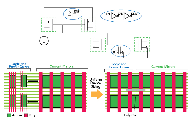
Figure 4 Benefits of uniform device sizing.
ESTIMATE INTERCONNECT PARASITICS FROM THE START
Analog designers generally introduce parasitic extraction only at a later stage of the design. They are included in schematic simulations only for high speed circuits and are limited to sensitive nets because resistance is rarely a problem. This approach does not work with FinFETs. Wiring and RC layout-related parasitics are, in many ways, the limiting factor for performance and these parasitics must be considered from a very early stage. Metal and via resistance are higher, making them more dominant factors than in a planar geometry. Running parasitic-extracted simulations that do not estimate resistance can give optimistic results and may result in a pointless exercise.
As analog blocks tend to use a limited number of transistor geometries, it is recommended to build a library of layouts for these devices. This library should include low-level vias and interconnects. After RC extraction, the resulting sub-cells can be used to design analog blocks. This will ensure that their RC components are included in the simulations from the start.
USE DIGITAL CALIBRATION TO CORRECT ANALOG ERRORS
FinFET lithography is extremely accurate, which should enable better component matching. However, the area of the components tends to be smaller than in planar geometries. Since device matching is inversely proportional to the square root of the device area, this can result in a large offset in comparators or a mismatch in mirrors.
Trying to address this problem by modifying device dimensions may be difficult, if not completely unsuccessful. FinFET logic gates are small and have low power. Wherever possible, it is prudent and much cheaper to resort to digital calibrations to remove matching errors.
CURRENT DENSITY LIMITS THE TRANSMITTER OUTPUT POWER
Designers have already faced this challenge when working on sub-40 nm planar geometries. However, FinFET skinny metal layers and small vias impose even more stringent limitations on the maximum current density. These layers and vias have limited current carrying capability. This may force power amplifier (PA) designers to use wider wires and increase the transistor width to accommodate the required vias and contacts. Depending on the voltage levels, designers may also need to increase the wire spacing.
Longer wires and larger gate areas introduce parasitics, making interconnects one of the limiting factors in PA design. The effects of interconnects must be considered in conjunction with the usual efficiency and linearity trade-offs. Surprises can be avoided by floor planning the amplifier early in the design phase, even when the desired output power is relatively modest and on the order of just a few milliwatts.
HIGH FLICKER NOISE CORNER FREQUENCY
Flicker noise in FinFET devices is a bigger issue than in planar geometries and the corner frequency in this architecture can be as high as 100 MHz. The impact on noise-sensitive circuits like VCOs, PLLs and receiver amplifiers can be very significant. The obvious solution to this issue is to increase the size of the devices. This will reduce the noise, but this improvement comes at the expense of RF performance. Alternatively, some of these issues can be resolved at the system level. For example, careful receiver frequency planning can ensure baseband operation at frequencies above the flicker corner and relax the associated block-level specifications.
SIMULATIONS ARE SLOW
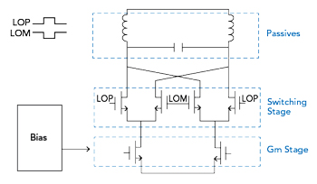
Figure 5 Hierarchy of a Gilbert cell mixer optimized for FinFET simulation.
FinFET models are complex, which leads to slow simulations. In addition, since the parasitic resistance cannot be ignored, most of the simulations will be performed with an extracted netlist that includes thousands of components. This can result in a brute-force approach that relies on big servers and multi-core simulators to thoroughly evaluate and verify the design. However, a better recommendation is to adapt the simulation strategy to this challenge and increase the hierarchical levels in the design. As an example of this methodology, Figure 5 proposes a more structured hierarchy for a simple Gilbert cell mixer. Given the limited number of components, the whole circuit could be drawn flat. However, after layout extraction, this choice leads to a large, flat netlist, with limited simulation and debugging options.
On the other hand, a more granular hierarchy like the one shown in Figure 5 separates the different sections of the design based on their functionality. Depending on the simulation, this gives the designer flexibility to use accurate, fully extracted views for critical sub-blocks while using coarser models for the other sections. As a rule of thumb, most block-level simulation times should be kept under one hour in duration. This limits the brute-force tests to the final verification stage.
CONCLUSION
FinFET device architectures have many advantages for large MIMO antenna-based RF systems. The architecture enables small, high speed digital signal processing to integrate into flexible digital radios. However, the expansion of RF applications into higher frequency bands means that the power consumption performance of RF ADC/DAC-based solutions becomes a serious challenge. One approach to minimize this challenge is to design low-power RF analog front-ends to convert the high frequency RF signal to a lower frequency IF signal. Realizing high performance, cost-effective approaches for this conversion process and circuitry will be of paramount importance to the success of these systems. Moving to FinFET technology represents a drastic change for analog designers, but this article has presented seven recommendations to smooth this transition and facilitate high performance FinFET analog circuit design.