

Spectral Error
The linear FM (LFM) waveform (chirp) is composed of discrete frequency points. There is a distribution error between frequency points. The spectral interval of the chirp is df. The spectral distribution error coefficient is β. This model uses a uniform distribution error βdf for the spectral distribution error and compares the effect of the uniform spectral distribution error on image quality (See Figure 9).
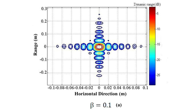
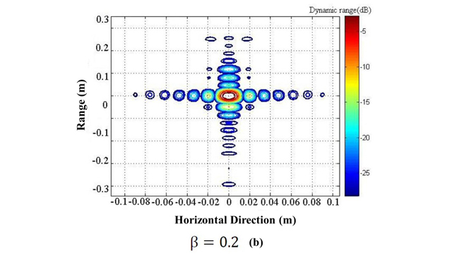
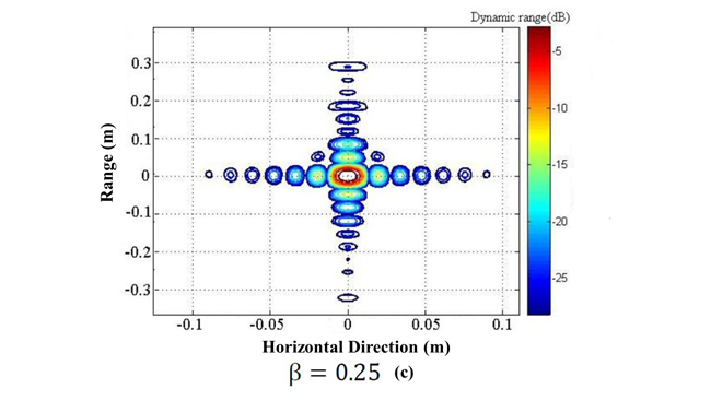
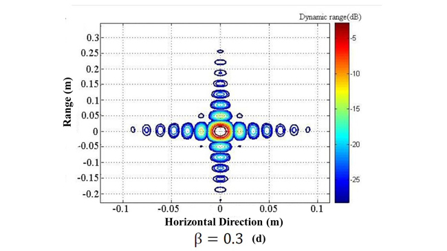
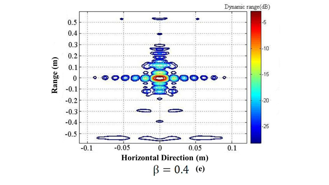
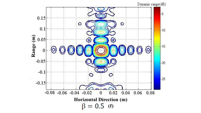
Figure 9 The effect of spectral error on image resolution: β = 0.1 (a), β = 0.2 (b), β = 0.25 (c), β = 0.3 (d), β = 0.4 (e) and β = 0.5 (f).
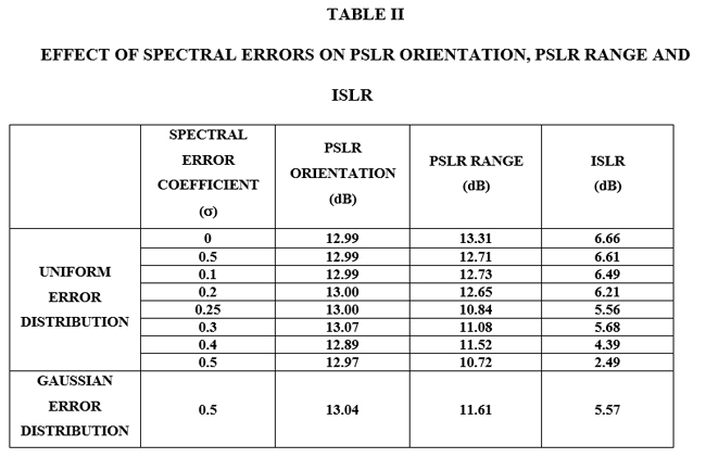
The effects of a uniform distribution and a Gaussian spectral distribution error on PSLR orientation, PSLR distance and ISLR are shown in Table II. The image starts to demonstrate obvious distortion with uniform distribution error (−0.2df, 0.2df) with an increase in ISLR.
Compared with the array error, the spectral error has a greater impact on imaging. Sidelobes are increased and with greater energy leakage. Therefore, the device has higher requirements for spectral error. To ensure the imaging accuracy, spectral error should be less than 10 percent.
Linearity
Linearity (L) is an important measure of RF source quality; it directly affects measurement accuracy and resolution.
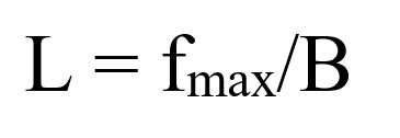
where fmax is the maximum frequency deviation and B is the bandwidth. For this system, B = 5 GHz for an ideal range resolution of 3 cm.
Generally, a LFM signal deviates from linearity by fluctuating around the ideal frequency with a periodicity assumed to be a single-frequency cosine:

The actual signal is the sum of an ideal linear signal and this error signal, i.e:
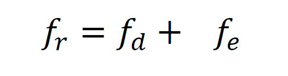
Figure 10 shows the simulation results, in which a linearity of about 5*e−4 has little effect on imaging.
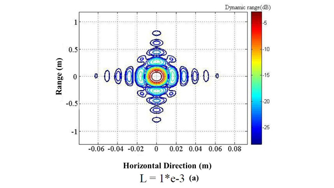
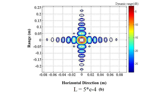
Figure 10 The effect of source linearity on imaging quality: L = 1e-3 (a), L = 5e-4 (b) and L = 1e-4 (c).
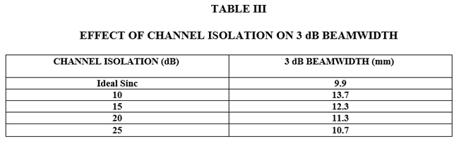
EFFECT OF CHANNEL ISOLATION ON IMAGE RESOLUTION
RF channel isolation is an important indicator of antenna array and RF module performance. If isolation is low, crosstalk, amplitude error and phase error will affect image resolution. Figure 11 shows that poor channel isolation results in a decrease in the proximal paralobe, elevation of the distal paralobe, and widening of the main lobe. Table III shows the effects of channel isolation on 3 dB beamwidth. When isolation is 25 dB, image resolution is greatly improved. Because there are additional errors in antenna array processing, to achieve an overall isolation of greater than 25 dB, component isolation is specified to be 40 dB.
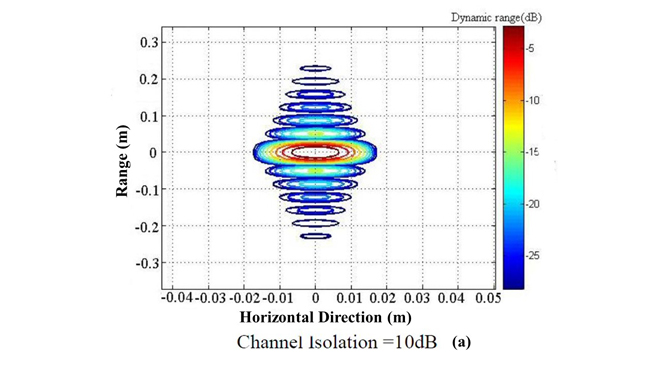
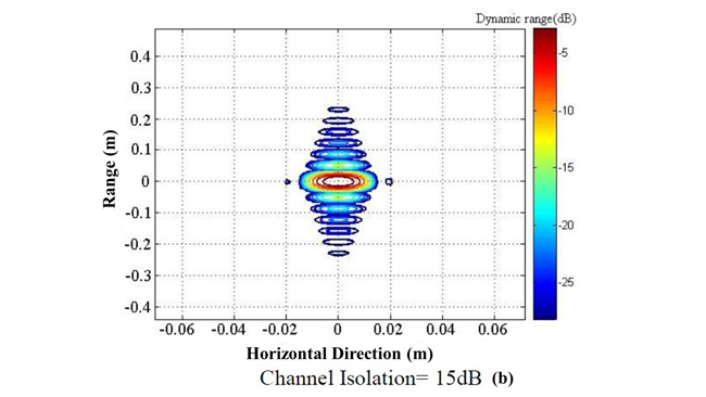
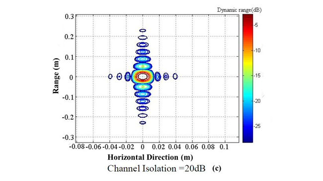
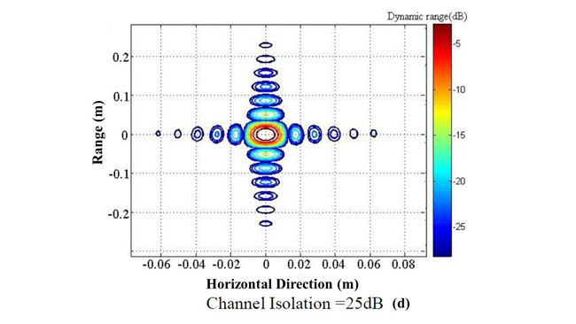
Figure 11 The effect of channel isolation on imaging quality: channel isolation = 10 dB (a), 15 dB (b) 20 dB (c) and 25 dB (d).
IMAGING SYSTEM COMPOSITION
The main components of the MMW imaging system include an RF system, an acquisition system, a scanning system, a control board and a computer system (see Figure 12). The control panel and sequential controller (control board) determine the status of the RF and acquisition systems. When the scanning system moves to a specific position, the transmit antenna array in the RF system sends out a mmWave signal that is reflected and received by the receiving antenna in the same position. The received signal is converted to an intermediate frequency (IF) in the RF system and the acquisition system collects the IF signal for processing and analysis. The output is a baseband signal transformed and displayed as an image by the computer system.
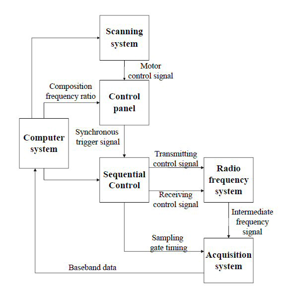
Figure 12 mmWave 3D imaging system.
Figure 13 is a block diagram of the Ka-band transceiver desktop module (the Radio Frequency System in Figure 11). It produces the wideband linear frequency modulation signal, 192 and 100 MHz synchronous reference signals and send/receive array switch control signals. It receives the weak signals from the antenna and provides signal amplification, mixing, filtering processing and I/Q outputs. A photo with some of the key components is shown in Figure 14.
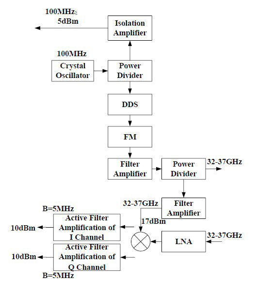
Figure 13 Ka-band transceiver block diagram.
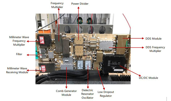
Figure 14 Ka-band transceiver photograph.