

Filters are routinely used in microwave frequency converter modules to channelize signals. Since most applications require multiple filters, size becomes a critical design parameter, particularly for filters in the L- and S-Band range where printed filters are desirable but can be large and can quickly use up the available area within a module. Interdigital filters are a good choice due to the topology’s inherent size efficiency, but to significantly reduce filter area, a method of stacking filters is also needed. This article presents a strategy using Multi-Mix® technology for stacking filters in a common footprint, enabling optimal size reduction in converter modules. Multi-Mix® is a patented technology developed at the Merrimac Industries location of Crane Aerospace & Electronics.
INTERDIGITAL FILTERS
The interdigital filter topology is compact, making it useful to reduce filter size at low microwave frequencies. Small size is the benefit, but there are significant tradeoffs with ease of implementation and sensitivity to resonator grounding. The typical implementation of a printed interdigital filter uses plated through via holes or plated through slots to ground the resonators. The associated reactance of the grounding geometry detunes the filter from the synthesized dimensions, but this can be overcome by using available analysis software to optimize performance and overdesign the bandwidth and selectivity for variations in dielectric constant (εr), substrate thickness and etching tolerance.
Using a filter synthesis tool, an initial model can be generated that includes the representative Q of materials. This is where the overdesign begins so that real-world variations can be absorbed into an approach that requires no tuning. A wider passband must be incorporated into the design to allow for a shift in center frequency and about 10 dB of additional close-in rejection should be built into the selectivity of the model by choosing a filter of sufficient order. A representative schematic is shown in Figure 1a for an optimized model of an interdigital filter.
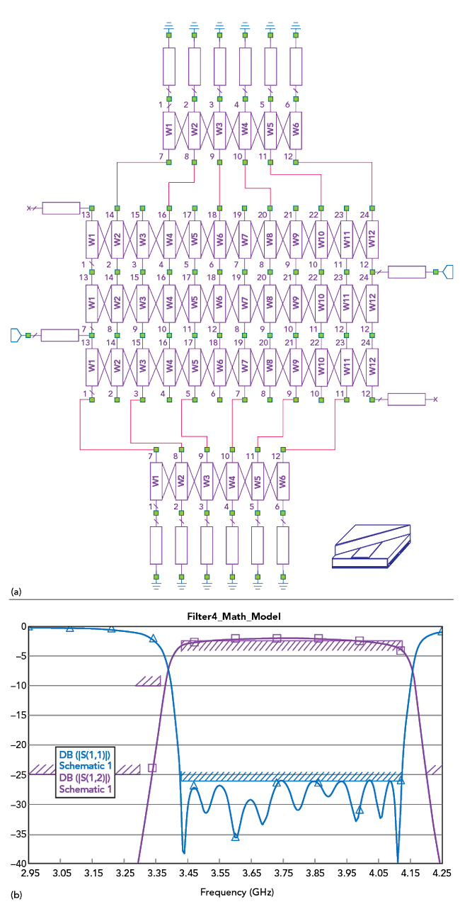
Figure 1 (a) Schematic of an optimized model for an interdigital filter. (b) Frequency response of an optimized model for an interdigital filter.
Optimization of the initial synthesis model is always required due to the representative features of resonator grounding. The corresponding frequency response of the optimized model is shown in Figure 1b. The layout generated by the model is used to build the physical 3D electromagnetic (EM) model of the interdigital filter.
Figure 2a shows a typical HFSS model representation of an interdigital filter. In the illustration, multiple filters are shown in the multilayer, fusion-bonded stripline module, but the initial EM modeling should be isolated to a single filter to capture the variation with dielectric constant, ground plane spacing and etching tolerance of resonator line widths and gaps. The corresponding nominal frequency response of the EM model is also shown in Figure 2b.
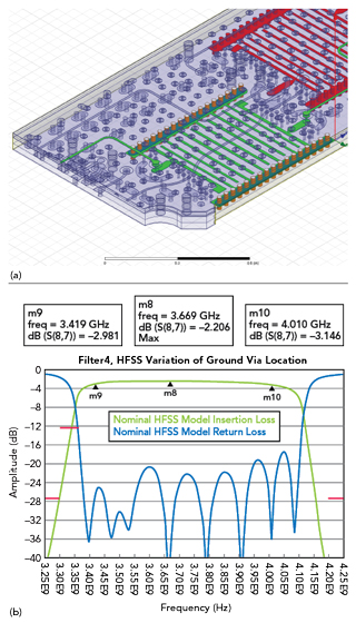
Figure 2 (a) Physical 3D interdigital filter electromagnetic model. (b) Frequency response of the interdigital filter EM model.
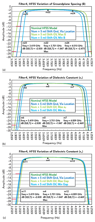
Figure 3 (a) Passband response of the 3D EM model showing variation due to ground plane spacing. (b) Passband response of the 3D EM model showing variation due to dielectric constant. (c) Passband response of the 3D EM model showing variation due to etching tolerance.
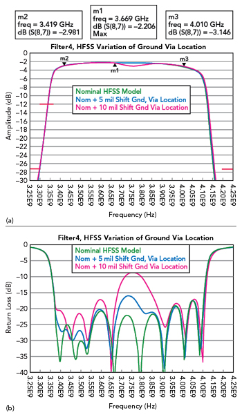
Figure 4 (a) HFSS model showing the effect of axially shifted ground vias on amplitude. (b) HFSS model showing the effect of axially shifted ground vias on return loss.
The EM model can be used to bracket the worst-case performance variation so that it can be determined if the effects of material and manufacturing tolerance can be absorbed, or if they need to be mitigated. Figure 3a shows the passband response of the 3D EM model with ground plane spacing due to the dielectric material thickness tolerance (B = 0.060 ± 0.003 in.) Figure 3b shows the effects of substrate material dielectric constant tolerance (εr = 3 ± 0.04) and Figure 3c shows the etching tolerance of resonator line width and gap dimensions due to manufacturing processes (± 0.0005 in.). The performance variation due to dielectric material thickness affects the ground plane spacing and consequently, bandwidth. This variation is usually too extreme to be absorbed into a no-tune design. The dielectric thickness tolerance of laminate material ranges from ± 0.001 to ± 0.003 in. A typical tolerance of ± 0.0015 in. produces a substantial change in bandwidth as a thicker ground plane spacing widens the band and a thinner ground plane spacing narrows the band. Usually, the close-in rejection requirements cannot tolerate this variation, so the mitigation is accomplished by measuring and selecting layers by thickness within a tighter tolerance.
Several different circuits may be required to match the material availability, but the layer thickness should be specified and measured before fabrication. The performance variation, due to material dielectric constant, is usually absorbed into a design at lower microwave frequencies in L- and S-Bands. If this variational parameter requires mitigation for higher frequency designs or tighter frequency tolerances, there are two options. The dielectric constant for a given material lot is very consistent, so the baseline design for εr = 3 can be run for each new material lot and if required, the circuit may be iterated to compensate for a particular lot. Alternately, several designs can be included on a panel array with resonators slightly longer and shorter to coincide with the increase or decrease in center frequency due to the variation in εr. This ensures there will always be some yield for this test panel. For that lot of material, this procedure will identify the best circuit to use for the balance of the filter production. The performance variation due to the etching tolerance of resonator line width and gap dimensions is small for a 0.0005 in. tolerance, so that variation is usually absorbed into the design.
The greatest challenge in fabricating a printed interdigital filter is in the drill-to-pattern registration. The typical manifestation of this variation is an axial shift of the via hole pattern that grounds the resonators. The shift is in one direction along the centerline of the resonators of the printed filter pattern. A visualization of this phenomenon can be seen in the HFSS model of Figure 2a, where the ground vias all shift in the minus X direction. In this case, the interdigital resonators get longer on one side of the filter and shorter on the other side. This shift, alternating between longer and shorter, causes a VSWR hump in the middle of the band. The effect of the axial via shift is shown in the amplitude versus frequency response of Figure 4a and the return loss versus frequency response of Figure 4b. The effect is more sensitive than most analysis software will predict. For example, depending on the specific filter characteristics (order, frequency, bandwidth, etc.), the magnitude of the VSWR effect shown in Figure 4a for a 0.010 in. axial shift in ground vias will more likely occur at a much smaller value of axial shift. A good goal is to keep drill-to-pattern variation within 0.002 in. Fortunately, direct imaging technology can be used to register each filter image in the array to be aligned to the actual via pattern that is drilled and plated on the substrate panel.
STACKED FILTERS
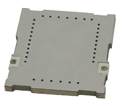
Figure 5 2.9 GHz fusion-bonded, surface-mount filter.
Stripline interdigital filters can be implemented as a fusion-bonded assembly of etched circuits with plated through holes, edge-plated (wrapped) grounding and surface-mount interface connections. The fusion bonding process for stacked filters begins with commercially available PTFE composite, copper-clad laminate material having inherently low dielectric loss and stable microwave properties. A low z-axis coefficient of thermal expansion (CTE), close to that of copper, ensures the reliability of plated through holes, along with blind and buried vias. Further, a low and uniform thermal coefficient of dielectric constant, coupled with the low CTE, results in consistent electrical performance over a wide operating temperature range. Stripline filter circuit patterns and transmission line geometries are chemically photo etched on the copper, maintaining dimensional tolerances of ± 0.0005. Layer-to-layer plated through holes (blind and buried vias) are realized with a minimum diameter of 0.005 in. Properly sized and spaced blind and buried vias are used throughout the layers to create matched impedance structures that connect between layers and through interstitial ground planes. These vias also isolate lines and filter structures within a ground plane. The ability to achieve a high degree of isolation within a given layer allows further size reduction and the elimination of unwanted resonances. Fusion bonding is accomplished by stacking the panels of the arrayed filter layers in a fixture. Carefully controlled, uniform pressure and temperature are applied to this fixture to meet the substrate fusion bonding requirements. After fusion bonding, the stacked filters are edge-plated with copper for EMI shielding and ground plane integrity and then finished with annealed matte tin, tin/lead or nickel/gold, depending on the application.
The operating frequency range of this stacking strategy has been demonstrated from Very High Frequency through Ka-Band, but an essential element of the strategy that allows for success is EM modeling. EM modeling of the full filter layout is important since there will be no opportunity to tune the bonded assembly. To accurately predict the expected performance, the full filter model should also be evaluated in its final form, mounted to a parent board as it would be in the integrated module assembly. A photo of an actual 2.9 GHz fusion-bonded filter is shown in Figure 5 with outline dimensions of 0.75 × 0.75 × 0.07 in. Test data for this filter is plotted in Figure 6, showing less than 3 dB of insertion loss and greater than 15 dB of return loss over a 1 GHz bandwidth.