Pseudomorphic high electron mobility transistors (PHEMT) have shown excellent microwave and noise performance and are very attractive for millimeter-wave and optoelectronic applications. The complete characterization of these devices, in terms of noise and scattering parameters, is necessary for computer-aided design (CAD) of monolithic microwave integrated circuits (MMIC) or optoelectronic integrated circuits (OEIC).1–3 The full noise characterization of a PHEMT requires the determination of four noise parameters: minimum noise figure Fmin, noise resistance Rn, optimum source conductance Gopt and optimum source susceptance Bopt. The determination of the noise parameters is typically performed by analyzing the variation of the measured noise figure as a function of the source impedance. A minimum of four independent measurements is required. However, for increasing accuracy, more than four measurements are usually performed and curve-fitting techniques are then used to determine the noise parameters.4–7 Several authors8–10 have proposed improved methods, using the equivalent transistor noise model, to provide additional information to reduce the complexity of the measurement procedure. The noise models can be broadly obtained by numerical and experimental approaches, both of which could lead to an equivalent-circuit representation with adequate parameterization. These measured noise parameters can be coupled with S-parameter measurements into an equivalent-circuit model, an approach that is common for microwave devices.11–16 An empirical relation between the noise figure and the circuit parameters, employing fitting parameters, was proposed for GaAs FETs by Fukui.12 More quantitative equivalent-circuit modelings have been pursued by Statz, et al.13 and Pospieszalski,14 where the noise was equivalently represented as gate and drain temperature or resistance/conductance using Nyquist noise sources.

In order to optimize the noise performance of PHEMTs for low noise applications, fully scalable analytical expressions for the noise parameters, which can provide good accuracy and be scalable based on the layout structure as well as gate width, are very attractive for MMIC design and have a number of advantages. These advantages include:
-
The noise parameters of different size devices using the same process can be readily obtained using scalable normalization model parameters, so low cost and time savings can be achieved
-
They are useful for understanding the physical mechanisms and for evaluating the influence of the different parameters of the small-signal equivalent circuit model
A. Cappy derived simple analytic expressions for the minimum noise figure, noise conductance and the optimum source impedance based on an equivalent circuit, considering only the intrinsic gate-to-source capacitance and extrinsic gate and drain resistances.17 Unfortunately, fully scalable analytical expressions for the noise parameters have not been discussed yet. In this article, a set of new expressions for the four noise parameters of AlGaAs/InGaAs/GaAs PHEMTs are derived from an accurate noise equivalent circuit model without any assumptions and approximations. The effects of all intrinsic elements and gate leakage current are taken into account. The scaling rules for the noise parameters of intrinsic part are determined, based on these analytical expressions.
Theoretical Analysis
Device Structure
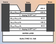
The AlGaAs/InGaAs/GaAsPHEMT with 0.25 μm mushroom gates have been grown and fabricated using Nanyang Technological University’s (NTU) developed process technology. The layer structure of the wafer, from bottom to top, consists of a GaAs undoped buffer layer, a 140 Å undoped In0.22Ga0.78As strained layer, a 40 Å Al0.25Ga0.75As spacer layer, a 5 × 1012cm–2 Si δ-doping plane, a 220 Å I–Al0/25Ga0.75As source layer and a Si-doped 450 Å n+–GaAs cap layer. Here, a PI-gate PHEMT has been used, which has a 2 × 40 mm gate width (number of gate fingers × unit gate width) and a pinch off voltage of approximately –0.8 V. The double heterojunction δ-doped PHEMT structure considered in this study is shown in Figure 1. Figure 2 shows the layout of the interdigitated double heterojunction δ-doped PHEMT.

Noise Model
From the circuit point of view, the FET device can be treated as a black box of a noisy two-port. As is well known, the noise behavior of a linear noisy two-port network can be characterized by the four noise parameters, Fmin, Rn, Gopt and Bopt, with

where
F = noise figure
Ys = Gs + jBs = source admittance
Fmin = minimum noise figure
Rn = noise resistance
Ys = Gs + jBs = optimum source admittance
The complete PHEMT small-signal and noise equivalent circuit model, including the intrinsic and extrinsic parts, is shown in Figure 3. The circuit model comprises the well-known small-signal equivalent circuit, and six noise sources ![]() and
and ![]() . The three noise sources
. The three noise sources ![]() represent the noise behavior of the access resistances Rg, Rd and Rs, and are simply given by:
represent the noise behavior of the access resistances Rg, Rd and Rs, and are simply given by: ![]() = 4kTRiΔf, where k is the Boltzmann constant, T is the absolute temperature, Ri is the resistance value and Δf is the bandwidth. The two correlated current noise sources
= 4kTRiΔf, where k is the Boltzmann constant, T is the absolute temperature, Ri is the resistance value and Δf is the bandwidth. The two correlated current noise sources ![]() and
and![]() represent the internal noise sources of the intrinsic PHEMT. These two noise sources are characterized by their mean quadratic value in a bandwidth Δf centered on the frequency f, and can be given by the following expressions1
represent the internal noise sources of the intrinsic PHEMT. These two noise sources are characterized by their mean quadratic value in a bandwidth Δf centered on the frequency f, and can be given by the following expressions1

The cross correlation between ![]() and
and ![]() can be expressed as
can be expressed as
![]()
where R and P are the gate and drain noise model parameters, and C is the correlation coefficient.
![]() represents the gate leakage current noise source, and is given by18,19
represents the gate leakage current noise source, and is given by18,19
![]()

where
IgL = gate leakage current
α = fitting factor
In the small-signal and noise equivalent circuit model, Lg, Ld and Ls represent the inductances of the gate, drain and source feed-lines, respectively, Cpg, Cpd and Cpgd represent the gate, drain and isolation between gate and drain pad capacitances, Rs and Rd are the source and drain resistances, Rg is the distributed gate resistance, Cgs, Cgd and Cds are the gate-to-source, gate-to-drain and drain-to-source capacitances, respectively, and Ri is the channel resistance. gm is the transconductance, gds is the drain conductance and τ is the time delay associated with transconductances.
Derivation of the NOise PARAMETERS
New Expressions for the Noise Parameters
From the intrinsic part of the small-signal model, it can be found that it consists of seven elements: gm, gds, Cgs, Cgd, Cds, Ri and τ. The corresponding short circuit Y-parameters of the intrinsic small-signal equivalent circuit can be expressed as20


The corresponding admittance noise correlation matrix can be expressed as

where VT represents the thermal voltage (VT = kT/q).
Based on the noise correlation matrix technique,21 the four noise parameters can be directly calculated from the chain noise correlation matrix
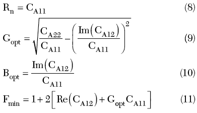
where

with Equations 5 and 6 substituted in Equations 7 to 10, one gets
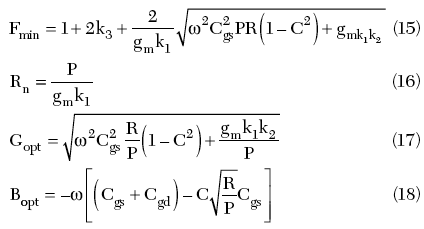
where

Scaling Rules
According to the scaling rules of PHEMTs, the intrinsic small-signal model parameters have a standard scaling:22 the intrinsic capacitances, transconductance and output conductance are proportional to the gate width and the intrinsic resistance is inversely proportional to the gate width, that is

where n represents the number of the elementary cells for the larger gate width size device, which is defined by

and the superscript c denotes the elementary cell.
Assuming that the time delay remains invariant at the same bias condition for the same device process, that is τ = τc, with Equation 18 substituted in Equation 5, one gets
![]()
From Equation 20, it can be found that a large gate width size PHEMT can be viewed as consisting of n elementary cells with the same gate width connected in parallel. Based on the noise correlation matrix technique,21 the admittance noise correlation matrix for a large gate width size PHEMT can be expressed as
![]()
Because the gate leakage current is not scalable, all the scaling rules for the noise parameters n this article will not include the effect of gate leakage current (dashed box in the intrinsic part of the noisy small-signal equivalent circuit model). With Equations 18 and 21 substituted in Equation 6, one gets

With Equations 22 to 24 substituted in Equations 14 to 17, it can be found that the scaling rules of the noise parameters for the intrinsic part are as follows: the minimum noise figure Fmin remains invariant, the noise resistance Rn is inversely proportional to the number of elementary cells, and the optimum source conductance Gopt and the optimum source susceptance Bopt are proportional to the number of the elementary cells, that is

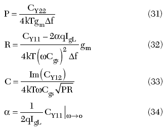
Determination of Noise Model Parameters P, R, C and α
Once the small-signal elements are extracted from the S-parameter measurements, the extraction of the four unknown noise model parameters can be carried out using the procedure based on the noise correlation matrix technique as follows23
1. Calculation of the chain noise correlation matrix for PHEMT.

2. Transformation of the chain noise correlation matrix to the admittance noise correlation matrix and subtraction of pad capacitances (Cpb, Cpc and Cpbc). Because the pad network is a noiseless network, the admittance noise matrix remains invariant.
3. Transformation of the admittance noise correlation matrix to the impedance noise correlation matrix and subtraction of extrinsic inductances and resistances.
4. Transformation of the impedance noise correlation matrix to the impedance noise correlation matrix.
The noise model parameters can then be determined as
Experimental Verification

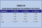
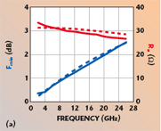
In order to verify the equations derived for the four noise parameters, 0.25 μm AlGaAs/InGaAs/GaAs double heterojunction δ-doped PHEMTs, with 2 × 20 μm, 2 × 40 μm and 2 × 60 μm gate widths, have been characterized. The S-parameters for model extraction and verification were measured up to 40 GHz using an Agilent 8510C network analyzer. The DC bias was supplied by an Agilent 4156A. The microwave noise parameter measurements were carried out on wafer over the frequency range of 2 to 26 GHz using an ATN microwave noise measurement system NP5. The extracted values of the bias-independent small-signal elements for the 2 × 20 μm, the 2 × 40 μm and the 2 × 60 μm PHEMTs are summarized in Table 1. Once the values of the parasitic elements are known, all bias-dependent elements can be easily determined by using a direct extraction technique.22 The corresponding intrinsic parameters gm, τ, Cgs, Cgd, Cds, Rbi and gds at a constant drain-source voltage Vds = 2.0 V and Ids = 6 mA, 12.2 mA, and 18 mA for 2 × 20 μm, 2 × 40 μm and 2 × 60 μm PHEMTs are given in Table 2. It can be observed that the time delays τ are nearly constant for different size devices. The extracted noise model parameters P, R, C and α are summarized in Table 3. It can be found that P, R and C remain invariant for four different gatewidth size PHEMTs under the same bias condition. However, the gate leakage current cannot be scalable. The measured and computed noise parameters versus frequency are compared in Figure 4 for a 2 × 20 μm PHEMT under the single bias conditions Vgs = 0 V, Vds = 2 V. A good agreement is observed. The new expressions are also compared with the model proposed by A. Cappy17 (green lines). The red lines correspond to the values calculated from Equations 14 to 17. The new expressions are clearly more accurate than Cappy’s. Because of the gate leakage current effect, the minimum noise figure does not cross the zero point. To illustrate the efficiency of the scaling rules for noise parameters, the measured and predicted results for larger size PHEMTs (2 × 40 μm and 2 × 60 μm) are compared in Figure 1 and 6. The 2 × 40 μm and 2 × 60 μm PHEMTs can be viewed as consisting of two and three elementary cells (2 × 20 μm PHEMT) connected in parallel. The measured data for the intrinsic part of the 2 × 40 μm and 2 × 60 μm PHEMTs are obtained after de-embedding the extrinsic elements from the measured noise parameters and the predicted data are obtained via the scaling process (Equations 25 to 28) from the elementary cell (2 × 20 μm PHEMT). Good agreement is obtained between measured and predicted data to validate the scaling approach for noise parameters.
Conclusion
In this article, a set of new analytical expressions for the noise parameters of PHEMTs in the microwave frequency range is proposed. These expressions are derived on the basis of an accurate small-signal and noise equivalent circuit model. The scaling rules for the noise parameters are determined for different gatewidth PHEMTs under the same process condition. The experimental and theoretical results show that for the same bias conditions, good scaling of the noise parameters can be achieved between the large-size device and the elementary cell.

References
1. H. Ikeda, T. Ohshima, M. Tsunotani, T. Ichioka and T. Kimura, “An Auto-gain Control Transimpedance Amplifier with Low Noise and Wide Input Dynamic Range for 10 Gb/s Optical Communication Systems,” IEEE Journal of Solid-State Circuits, Vol. 36, No. 9, September 2001, pp. 1303–1308.
2. Q.Z. Liu and R.I. MacDonald, “Sensitivity Analysis of Integrated InGaAs MSM-PDs and HEMT Optoelectronic Receiver Array,” IEEE Transactions on Electron Devices, Vol. 42, No. 7, July 1995, pp. 1221–1226.
3. N.R. Das, P.K Basu and M.J. Deen, “A New Approach to the Design Optimization of HEMT and HBT for Maximum Gain-bandwidth of MSM-based Integrated Photoreceiver and its Noise Performance at 1.55 mm,” IEEE Transactions on Electron Devices, Vol. 47, No. 11, November 2000, pp. 2101–2109.
4. R.Q. Lane, “The Determining of Device Noise,” IEEE Proceedings, Vol. 57, 1969, pp. 1461–1462.
5. G. Caruso and M. Sannino, “Computer-aided Determination of Microwave Two-port Noise Parameters,” IEEE Transactions on Microwave Theory and Techniques, Vol. 26, No. 9, September 1978, pp. 639–642.
6. A.C. Davidson, B.W. Leake and E. Strid, “Accuracy Improvements in Microwave Noise Parameter Measurements,” IEEE Transactions on Microwave Theory and Techniques, Vol. 37, No. 12, December 1989, pp. 1973–1978.
7. J.M. O’Callaghan and J.P. Mondal, “A Vector Approach for Noise Parameter Fitting and Selection of Source Admittance,” IEEE Transactions on Microwave Theory and Techniques, Vol. 37, No. 8, August 1989, pp. 1376–1382.
8. J. Gao, C.L. Law, H. Wang, S. Aditya and G. Boeck, “A New Method for PHEMT Noise Parameter Determination Based on 50 W Noise Measurement System,” IEEE Transactions on Microwave Theory and Techniques, Vol. 51, No. 10, October 2003, pp. 2079–2089.
9. M. Rudolph, R. Doerner, P. Heymann, L. Klapproth and G. Boeck, “Direct Extraction of FET Noise Models from Noise Figure Measurements,” IEEE Transactions on Microwave Theory and Techniques, Vol. 50, No. 2, February 2002, pp. 461–464.
10. R. Hu and S. Weinreb, “A Novel Wideband Noise Parameter Measurement Method and its Cryogenic Application,” IEEE Transactions on Microwave Theory and Techniques, Vol. 52, No. 5, May 2004, pp. 1498–1507.
11. G. Martines and M. Sannino, “The Determination of the Noise, Gain and Scattering Parameters of Microwave Transistors (HEMT) Using Only Automatic Noise Figure Test-set,” IEEE Transactions on Microwave Theory and Techniques, Vol. 42, No. 7, July 1994, pp. 1105–1113.
12. H. Fukui, “The Noise Performance of Microwave Transistors,” IEEE Transactions on Electron Devices, Vol. 13, No. 3, March 1966, pp. 329–341.
13. H. Statz, H.A. Haus and R.A. Pucel, “Noise Characteristics of Gallium Arsenide Field-effect Transistors,” IEEE Transactions on Electron Devices, Vol. 21, No. 9, September 1974, pp. 549–562.
14. M.W. Pospieszalski, “Modeling of Noise Parameters of MESFETs and MODFETs and their Frequency and Temperature Dependence,” IEEE Transactions on Microwave Theory and Techniques, Vol. 36, No. 1, January 1988, pp. 1–10.
15. F. Danneville, G. Dambrine and A. Cappy, “Noise Modeling in MESFET and HEMT Using a Uniform Noisy Line Model,” IEEE Transactions on Electron Devices, Vol. 45, No. 10, October 1998, pp. 2207–2212.
16. B.U.H. Klepser, C. Bergamaschi, M. Schefer, C.G. Diskus, W. Patrick and W. Bachtold, “Analytical Bias-dependent Noise Model for InP HEMTs,” IEEE Transactions on Electron Devices, Vol. 42, No. 11, November 1995, pp. 1882–1889.

Xiuping Li
17. A. Cappy, “Noise Modeling and Measurement Techniques,” IEEE Transactions on Microwave Theory and Techniques, Vol. 36, No. 1, January 1988, pp. 1–10.
18. D.S. Shin, J.B. Lee, H.S. Min, J.E. Oh, Y.J. Park, W. Jung and D.S. Ma, “Analytical Noise Model with the Influence of Shot Noise Induced by the Gate Leakage Current for Submicrometer Gate-length High-electron-mobility Transistors,” IEEE Transactions on Electron Devices, Vol. 44, No. 11, November 1997, pp. 1883–1887.
19. P. Heymann and H. Prinzler, “Improved Noise Model for MESFETs and HEMTs in Lower Gigahertz Frequency Range,” Electronics Letters, Vol. 28, March 1992, pp. 611–612.
20. G. Dambrine, A. Cappy, F. Heilodore and E. Playez, “A New Method for Determining the FET Small-signal Equivalent Circuit,” IEEE Transactions on Microwave Theory and Techniques, Vol. 36, No. 7, July 1988, pp. 1151–1159.
21. H. Hillbrand and P. Russer, “An Efficient Method for Computer-aided Noise Analysis of Linear Amplifier Networks,” IEEE Transactions on Circuits and Systems, Vol. 23, No. 4, April 1976, pp. 235–238.

Jianjun Gao
22. S.W Chen, O. Aina, W. Li, L. Phelps and T. Lee. “An Accuracy Scaled Small-signal Model for Interdigitated Power PHEMT up to 50 GHz,” IEEE Transactions on Microwave Theory and Techniques, Vol. 45, No. 5, May 1997, pp. 700–703.
23. R.A. Pucel, W. Struble, R. Hallgren and U.L. Rohde, “A General Noise De-embedding Procedure for Packaged Two-port Linear Active Devices,” IEEE Transactions on Microwave Theory and Techniques, Vol. 40, No. 11, November 1992, pp. 2013–2024.
Xiuping Li received her BS degree from Shandong University, P.R. China, in 1996, and her PhD degree from the Beijing Institute of Technology, P.R. China, in 2001. From 2001 to 2003, she was a research fellow in the Positioning and Wireless Technology Center, Nanyang Technological University, Singapore, where she was involved in the research and development of RFID systems. Her work in the MEMS group included micro-machined filter design and fabrication and coaxial and on-wafer measurements. She became a research professor at Yonsei University, Seoul, South Korea, in 2003, where she worked on 5 GHz WLAN/WMAN transceiver design. Since 2004, she has been an associate professor at the Telecommunication Engineering School of Beijing University of Posts and Telecommunications, P.R. China. Her main research interests include RF and microwave devices for communications, modeling and coaxial and on-wafer measurements.

Georg Boeck
Jianjun Gao received his B.Eng. and PhD degrees from Tsinghua University in 1991 and 1999, respectively, and his M.Eng degree from the Hebei Semiconductor Research Institute in 1994. From 1999 to 2001, he was a post-doctoral fellow at the Microelectronics R&D Center, Chinese Academy of Sciences, developing a PHEMT optical modulator driver. In 2001, he joined the School of Electrical and Electronic Engineering, Nanyang Technological University, Singapore, as a research fellow in semiconductor device modeling and on-wafer measurements. In 2003, he joined the Institute for High Frequency and Semiconductor Systems Technologies, Berlin University of Technology, Germany, as a research associate working on InP HBT modeling and circuit design for high speed optical communications. Since 2004, he has been a full professor at the Institute of RF & OE-ICs at Southeast University, Nanjing, China. His main research interests include characterization, modeling and on-wafer measurements of microwave devices, optoelectronic devices and high speed integrated circuits for optical communications.
Georg Boeck received his Dipl.-Ing. degree in electrical engineering and his doctoral degree from the Technishe Universität Berlin, Germany, in 1977 and 1984, respectively. In 1984, he joined the Siemens Research Laboratories, Munich, Germany, where his areas of research included fiber optics and GaAs electronics. From 1988 to 1991, he was a full professor of electronic devices and circuits at Fachhochschule Regensburg, Germany. Since 1991, he has been a full professor of microwave engineering at the Technishe Universität Berlin, Germany. His main areas of interest include characterization, modeling and design of microwave semiconductor devices, monolithic integrated circuits and MMICs up to the millimeter-wave range.
