Figure 5 (a) Coaxial line transformer model. (b) 3D model of the coaxial line transformer.
The Microwave Office schematic of a simple model of the coaxial line transformer used here is shown in Figure 5a. This model shows that the appropriate circuit elements are incorporated into the schematic. Figure 5b shows the full 3D model of the transformer with the Analyst simulator included within the Cadence AWR Design Environment. Figure 6 shows the simulated performance results of the schematic simulation and the full 3D analysis.

Figure 6 Simulated performance results of the coaxial transformer.

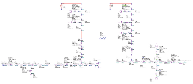
Figure 7 Complete PA schematic.
Complete PA Design
Pulling everything together, Figure 7 shows the complete schematic of the PA. Figure 8 illustrates the corresponding RF layout. Figure 9 shows the full printed circuit board (PCB) layout.

Figure 8 RF layout of the PA.

Figure 9 PCB assembly of the PA.

Figure 10 Simulated RF performance of the PA.
For this PA, typical design techniques were used for the matching/stabilizing and bias-decoupling networks. Figure 10 shows the simulated RF S-parameter and power added efficiency (PAE) performance at 60°C. Note that temperature is defined with respect to the bottom soldering plate of the transistor package.

Figure 11 Fundamental tone intrinsic load lines.
Figure 11 shows the I-V curves along with load lines at a few frequencies across the bandwidth at the intrinsic generator. In this case, only the fundamental tone is selected for simulation. Figure 12 shows these same I-V curves and load lines after simulating with 17 harmonics. Figure 12 shows the typical characteristics of a Class AB-biased transistor.

Figure 12 A depiction of the complex intrinsic load lines.
TEST RESULTS
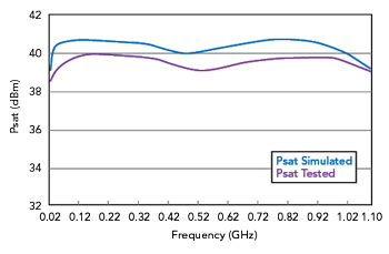
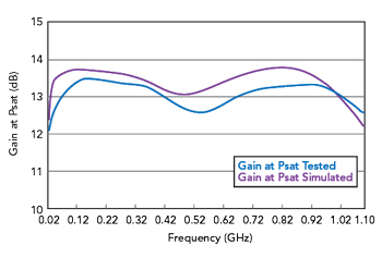
Figure 13 shows the simulated and measured small signal S-parameters. The results show that the simulated and measured S-parameters are in good agreement with each other. Figure 14 shows the simulated and measured saturated output power (Psat). The measured Psat is about 1 dB less than the simulated results, demonstrating a good overall result. Finally, Figure 15 presents the simulated and measured gain at Psat.

Figure 13 Simulated and measured small signal S-parameters.

Figure 14 Simulated and measured Psat.
Note that while it was not possible to accurately test PAE with the available test setup, it was estimated to be just above 40 percent. Figure 16 shows the prototype board and assembly that was used to test the PA.

Figure 15 Simulated and measured gain at Psat.

Figure 16 Prototype test circuit for the PA design.
CONCLUSION
The successful design of a multi-octave bandwidth PA, operating from 30 MHz to 1 GHz, using a 10 W, 50 V GaN HEMT from Qorvo, is demonstrated in this paper. The design used Modelithics models for all components. Good performance across this bandwidth can only be achieved by employing a coaxial line transformer with ferrite beads. This transformer must allow for an upward impedance transformation. To the authors’ knowledge, the use of such a transformer is presented for the first time in this paper. The transformer is simulated with the Analyst 3D FEM EM analysis tool within the Cadence AWR Design Environment. The design approach is based on the simulation of the load lines at the intrinsic generator. This simulation is possible because the Modelithics GaN transistor model lets the designer analyze the intrinsic voltages and currents. The full design is realized using Microwave Office software within the Cadence AWR Design Environment. The test results confirm that the design approach produces a first-pass success.
References
- I. Boshnakov, “A Simulation-Based Design Flow for Broadband GaN Power Amplifier Design,” High Frequency Electronics, March 2016, pp. 22–32.
- A. Grebennikov, “Power Combiners, Impedance Transformers and Directional Couplers,” High Frequency Electronics, December 2007, pp. 20–38.
