

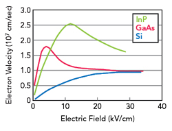
Figure 1 HBT electron velocities.
In the semiconductor RF world, indium phosphide (InP) heterojunction bipolar transistors (HBTs) have historically been a niche technology. High substrate costs and a lack of manufacturing expertise have contributed to limited adoption throughout the electronics industry. InP is, however, an ideal technology for many high speed electronic applications. With superior peak electron velocity compared to Si and GaAs and a higher breakdown voltage than SiGe, InP has the potential to benefit many microwave, mmWave and even terahertz (THz) applications. It has been used successfully in the electronic design, emulation and test industry for nearly two decades, enabling some of the highest performing instruments, including a 110 GHz real-time oscilloscope. Increasingly, InP HBTs are used or being considered for next-generation aerospace and defense, automotive and 5G/6G platforms. Capitalizing on the benefits of InP HBTs will require advanced packaging techniques to maintain high frequency performance and an industry-wide effort to reduce substrate prices.
INP HBT ADVANTAGES FOR RF DEVICES
Although the advantages of InP have been covered in many articles and white papers,1-3 ongoing research continues in both academia and industry to exploit the performance capabilities of this material for high frequency applications. InP’s most notable advantage is its electron velocity. This feature gives InP and its associated lattice-matched material systems, like indium gallium arsenide (InGaAs) or gallium arsenide antimonide (GaAsSb) an inherent advantage over other HBT device technologies. These systems can have peak electron velocities around 2.5 × 107 cm/s or higher, while GaAs-based systems have peak velocities of ~1.8 × 107 cm/s as shown in Figure 1. These peak velocities and the ability to engineer the transistor junctions with various material systems have resulted in a maximum frequency (fmax) greater than 1 THz with Arabhavi et al. reporting an fmax of 1.2 THz.4
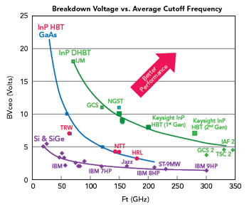
Figure 2 Breakdown voltage vs. cutoff frequency.
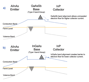
Figure 3 Type II band lineup with GaAsSb base (a). Type I band lineup with InGaAs base (b).
A second important advantage of InP is the ability to manufacture high breakdown voltage devices at high frequencies. For MMIC designs, the product of breakdown voltage between the collector and the emitter when the base is open (BVCEO) and cutoff frequency (ft) is a good metric for a semiconductor process. Higher BVCEO results in higher device power capabilities. The frequency where current gain goes to unity is ft and generally, the bandwidth of a MMIC increases with increasing transistor process ft. InP’s BVCEO × ft product is also a key advantage versus SiGe even though SiGe technology also produces devices exceeding 100 GHz. Cutoff frequency characteristics for various breakdown voltages are shown in Figure 2. While a 100 GHz SiGe circuit may have a breakdown voltage of ~1.6 V, a similar 100 GHz InP circuit can have a breakdown voltage of ~7 V.
Designing InP HBTs to capitalize on the breakdown voltage and speed advantages requires a process utilizing a heterojunction (an interface of two dissimilar materials) at the emitter-base junction and the base-collector junction. This is known as a double heterojunction bipolar transistor (DHBT). By carefully choosing the junction materials, bandgaps and band lineups, performance can be optimized for many applications. In an InP DHBT, a wide bandgap (1.35 eV) InP collector will provide a high breakdown voltage. In addition, as a binary material (two elements), it has better thermal properties compared to ternary material (three elements) alternatives.
A narrow bandgap material such as InGaAs (0.75 eV) or GaAsSb (0.72 eV) is typically used for the base. These materials, which have peak electron velocities like InP, enable a transistor turn-on voltage of typically ~0.6 V. This enables high frequency performance in situations where only low voltages are available. This can translate into lower heat dissipation and longer battery operation for handheld applications.
Compared to InGaAs, GaAsSb has the advantage of a Type II (staggered gap) conduction band lineup to the collector. This eliminates the electron barrier at the base-collector heterojunction, allowing for increased electron flow to the collector and higher collector current (Ic) as shown in Figure 3a and Figure 3b. With higher Ic, the amplification factor of the transistor (β= Ic/IB) increases, where IB is the base current. In addition, a paper from Iverson et. al. demonstrated an electron mobility of 1970 cm2/(V-s) for GaAsSb. The paper states, “For comparison, the value quoted for p-InGaAs in InGaAs/InP DHBTs at the same doping value was about 1500 cm2/(V-s).”5 That said, the InGaAs material system allows a higher doping and a lower base resistance, which allows for slightly higher frequency operation than GaAsSb.
Like the collector, the emitter also uses a wide bandgap material such as AlInAs or InP. By using an emitter material with a wide bandgap relative to the base, hole flow from the base to the emitter can be partially blocked by the bandgap discontinuity formed at the interface. This reduces IB, increasing β. With holes not materially participating in current flow across the emitter-base junction, higher doping of the base can occur, lowering the base resistance value and allowing for increased operating frequencies.
Another important note is that InP HBT technology simultaneously enables high frequency operation and high breakdown voltage while maintaining good broadband linearity and noise performance. This combination is key in the development of high frequency, broadband architectures.
INP HBT IN THE ELECTRONIC DESIGN, EMULATION AND TEST MARKET
The InP material system has enjoyed commercial success in the optical sector for nearly three decades. As a direct bandgap material with emission/detection > 1000 nm, InP-based devices have been used in telecom and datacom markets as laser diodes, modulators, photodiodes, mixers and more. In a 2019 Yole report outlining InP substrate use, telecom and datacom optical applications accounted for nearly 75 percent of an estimated $77 million market in 2018, while RF applications accounted for only 12 percent.6
In the RF sector, InP HBTs have been successful in the electronic design, emulation and test market. Figure 4 shows a representative InP HBT transistor structure. In 2012, Keysight’s predecessor, Agilent, shipped a 63 GHz oscilloscope.7 While this was not the company’s first oscilloscope utilizing InP (a 33 GHz model shipped a few years prior), it was the first oscilloscope that utilized the full capabilities of the InP HBT process, enabling a true 60+ GHz bandwidth front-end.
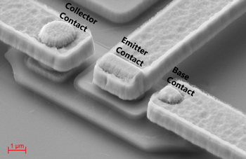
Figure 4 InP HBT SEM image.
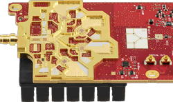
Figure 5 110 GHz oscilloscope front-end.
In 2018, Keysight used its second-generation InP HBT process to develop a 110 GHz real-time oscilloscope.8 By utilizing the high speed, broadband performance and high breakdown voltage of InP HBTs, Keysight designed an oscilloscope front-end with 110 GHz of analog bandwidth. This oscilloscope has exceptional noise performance and dynamic range without using frequency interleaving techniques that degrade signals. This oscilloscope front-end is shown in Figure 5. The scope utilizes six InP MMICs, including a 110 GHz pre-amp, a multi-GHz sampler and a limiting amplifier for NIST traceable calibration.
InP HBTs have also been used successfully in handheld analyzer applications. In 2008, Agilent introduced a new line of handheld RF analyzers with an example shown in Figure 6.9 Primarily targeted at installation and maintenance, these GaAs-based units operated up to 6 GHz without the need for fans or vents. The design challenge was to create a product with better performance that maintained the same portable form factor. Handheld products at higher bandwidths existed, but they compromised the handheld form factor by increasing the size, adding fans/vents and/or adding external heads for additional bandwidth coverage. Higher power consumption reduced battery life or required larger batteries to maintain the same operating time.
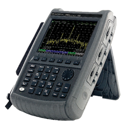
Figure 6 Microwave handheld analyzer.
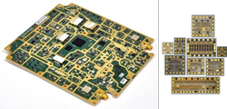
Figure 7 Handheld RF board (a) and associated InP MMICs (b).
In 2012, Agilent introduced an InP HBT-based unit operating up to 26.5 GHz.10 Utilizing the bandwidth and low turn-on voltage characteristics of the InP transistors enabled innovative design architectures. This allowed the high bandwidth models to fit the same handheld form factors as the lower bandwidth models. The RF board and associated InP MMICs are shown in Figure 7.