

To illustrate the working mechanism, an equivalent circuit model of the meta-resonator is shown in Figure 5. The interdigital structure is equivalent to a capacitor (Cr), and the equivalent inductor (Lr) comes from the inductance effect of the current loop (interdigital lines, metallic vias and the ground). Note that, different from the conventional SRR, the single-gap capacitor is replaced by an interdigital capacitor to obtain larger capacitance. A larger inductor is realized by using multiple thin metallic lines rather than a single metal structure.
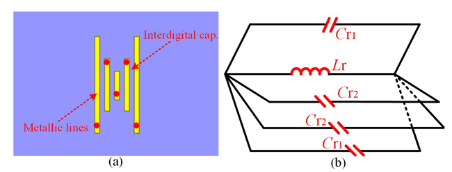
Figure 5 Bandstop meta-resonator: structure (a) and equivalent circuit (b).
The resonant frequency (fr) of this novel meta-resonator is derived by the following formula:

Thus, the resonant frequency can be flexibly tuned by controlling the equivalent capacitor (Cr) and/or inductor (Lr).
To verify the correctness of the equivalent circuit model, the meta-resonator structure is extracted separately, as shown in Figure 6. L1/L2 = L2/L3 = p11 is the length ratio of interdigital lines, d11 is the gap width between interdigital lines, and r1 is the radius of metal vias. As shown in Figures 6a and b, the larger p11, the higher the capacitance and the lower the resonant frequency. The opposite is true for d11. As shown in Figure 6c, the larger r1, the lower the inductance and the higher the frequency.
The transmission response of the meta-resonator is simulated in Figure 6d. A high-Q bandstop filtering characteristic at the working frequency (1.27 GHz) is observed. As a result, the original direct coupling path is suppressed and isolation between adjacent elements is further improved.
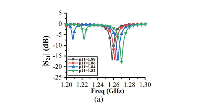
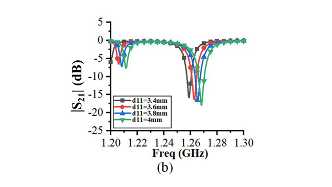
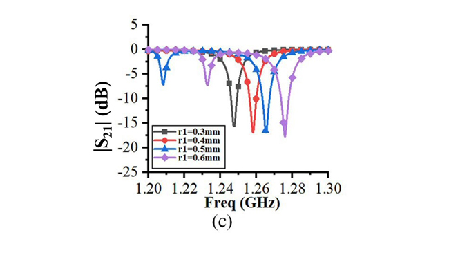
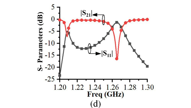
Figure 6 The relationship between p11 and bandstop frequency (a), the relationship between d11 and bandstop frequency (b), the relationship between r1 and bandstop frequency (c) and S-parameters of the meta-resonator structure (d).
The array with only a meta-resonator decoupling structure is analyzed (see Figure 7), showing that the decoupling effect is sensitive to p11 and d11. The trend is for a larger d11 and p11 to provide a lower |S21| but matching becomes worse.
Generally, CP array decoupling can be easily achieved by employing hybrid decoupling (i.e., both cancelation and suppression).
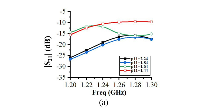
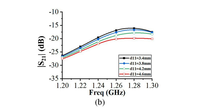
Figure 7 The relationship between p11 and |S21| (a) and the relationship between d11 and |S21| (b).
MEASUREMENT
The hybrid CP decoupling method is extended to a three-element array for fabrication and measurement (see Figure 8a). To verify radiation performance, the three-element CP array (P1/P3 matched, P2 excited) is measured in a far-field chamber (see Figure 8b). The measured 10 dB impedance band is wider than 1.25 to 1.28 GHz, which covers the Beidou B3 band, (see Figure 8c) and isolation is improved to better than 23 dB across the band (see Figure 8d).
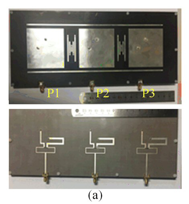
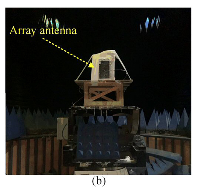
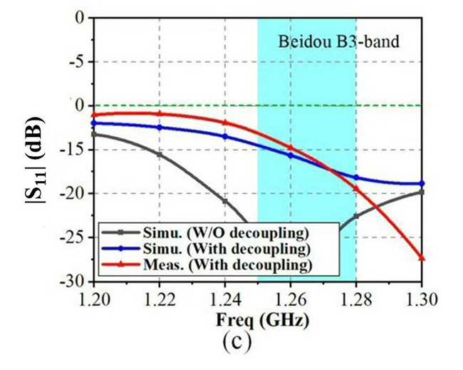
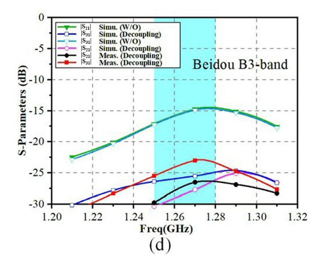
Figure 8 Photograph of the fabricated three-element closely-spaced CP array antenna (a), far-field chamber measurement setup (b) and S-parameters (c)(d).
The simulated and measured axial ratio (AR) bandwidth of the proposed array with and without decoupling is shown in Figure 9. The array antenna exhibits excellent CP radiation performance over a wider bandwidth after adding the decoupling structures. The measured 3 dB AR bandwidth is wider than 1.25 to 1.31 GHz, well covering the Beidou B3 band.
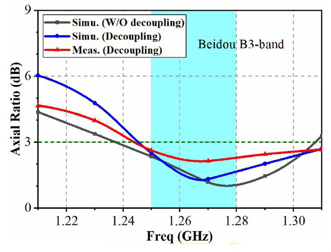
Figure 9 Measured and simulated AR bandwidth of the three-element closely-spaced CP array with P2 excited.