Microstrips (MS) and coplanar waveguides (CPW) are two of the main waveguide structures used in higher frequency applications, because of their compatibility with monolithic fabrication and solid-state devices. In CPW, the signal lines and ground planes are placed on one side of the substrate, permitting a circuit consisting of passive components and active devices to be implemented with relative ease. However, the most widely used lines are microstrips, which have the ground plane placed on the backside of the substrate. Consequently, a circuit element has to be connected through via holes for grounding.1 In many systems, it is necessary to use both type of lines simultaneously. A transition is required to connect them with minimum loss. This necessitates a common ground reference. At millimeter-wave frequencies, the presence of a backside metallization excites parallel plate waveguide modes. This problem leads to complex and costly solutions such as wafer thinning and backside processing in MMICs. In the case of CPW lines, the elimination of parallel plate modes requires a large number of vias, which introduce additional parasitic effects, increasing the circuit complexity. Therefore, the concept of a conductor-backed CPW2 is introduced, having the inherent advantage of lower radiation loss and higher power handling capability. The circuit can be viewed and analyzed as a system of three coupled slot lines. The transitions reported so far are limited by their length. This article introduces the concept of wideband, finite ground conductor-backed CPW (FG-CBCPW) lines, working from 19.5 to 22.0 GHz. This transition can be easily implemented in a monolithic configuration.
Modes in CBCPW Lines

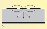
The backside metallization, in CPW lines, launches a microstrip-like mode. The dielectric thickness cannot be increased arbitrarily to minimize the effect of the backside metallization. In MMIC technology, the process limits the thickness, while the limitation in MICs comes from mechanical strength. Shih and Itoh have shown that the influence of the ground plane on the propagation characteristics can be significant when the substrate thickness becomes comparable to the slot width.3 Furthermore, the short circuit and discontinuities may cause parasitic modes, such as space waves and surface waves. Besides the parasitic radiation effect, the conductor backing may result in power leakage into the dielectric-filled parallel plates at all frequencies. The modes, which can exist in the metallized backside circuit, are the CPW mode, MSL (microstrip mode), first higher order microstrip mode and image guide-like mode, as shown in Figure 1.
The MSL mode can occur in a CPW with side planes of finite width, with or without conductor backing. The TM0 parallel plate mode, or surface mode, excited by discontinuities, may be converted into a bounded MSL mode. Thus, a CPW structure is overmoded. In this case, mode conversion among incident, transmitted and reflected waves takes place. The discontinuity between CBCPW and MS gives rise to the mode conversion process. In this mode, the electromagnetic energy is no longer confined in the vicinity of the CPW slot-surfaces; rather it may be carried by the microstrip-like mode, leaky wave, or other higher order modes, depending on the frequency of operation and the wave-guiding structures. Such non-CPW type of energy can couple to the neighborhood circuits and produces cross talk in the CPW circuit. The MSL mode, resembling the parallel plate transmission line mode, inherently exists in FW-CBCPW if no other means of mode suppression is applied. The next higher order MSL mode may exist if the side planes are too wide. The image guide-like mode exists if the substrate protrudes far from the side planes. It exhibits a zero cut-off frequency propagation characteristic.
The prevention of higher order modes in FG-CBCPW can be done by connecting the bottom ground to the side ground periodically with conducting posts. This configuration requires the conducting posts be placed near the conducting strips to form a quasi-rectangular waveguide beneath the strip operating below the cut-off frequency. However, this approach increases the circuit complexity. This article presents a novel transition structure, which eliminates the use of vias and ribbon bonds in addition to having a common ground reference. This makes the circuit simpler for ease of fabrication, along with a balanced configuration.
Broadbanding Technique

The bandwidth of a multi-section transformer can be increased by either having a binomial matching transformer for a flat response or a Chebyshev multi-section transformer to have further bandwidth improvement. A tapered line section has been used here, instead of a discrete line section to eliminate the effect of discontinuities.4 Figure 2 shows the tapering concept.
Z(z) = Z0 eaz 0 < z < L
where
α = (lnZL/Z0)/L
Using the theory of small reflections,
Γ = (lnZL/Z0) e–jβL sin βL/ βL
where
L = length of the taper
β = propagation constant
Furthermore, radial slots have been incorporated in the ground planes within the tapered section and further optimized. These slots present a very wideband open circuit, which forces the electrical field to be mainly in the microstrip line.
Design Aspects

The approach presented in this article combines the advantage of a single ground plane along with finite grounded coplanar (FGC) lines. The FGC lines provide the capability to control the cut-off frequency of the higher order modes, thus allowing higher operating frequencies. The finite size of the ground planes and the capability to change their size for controlling the performance is an added advantage of these lines. The ground plane is tapered in tune with the transition tapering. The width of the ground reference is chosen so that the lateral size of the structure is less than half the lowest operating wavelength. A common ground plane is chosen for the CPW and microstrip line, which is provided through the connectors. The single ground plane eases the circuit complexity as well as reduces the loss. In MIC fabrication, a single photolithography step is required for etching of the circuit. Radial slots, with an optimized angle of 45°, are incorporated for a wider bandwidth. The optimal width of the CPW is kept 2.5 times the distance between the two ground planes.3 The tapering section is designed to match 67 to 50 Ω. The widths of the CPW are kept as 24 mm for the signal line and 106 mm for the grounds. The spacing between the signal line and ground is kept at approximately 40 mm. These dimensions have been obtained after optimization of the transition length, spacing, width of the ground reference, tapering of ground reference along with slot length to achieve a wider bandwidth. The microstrip line width is kept at 0.24 mm.
Experimental Results

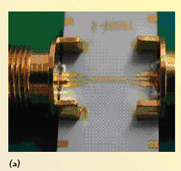
The circuit was simulated using the Microwave Office EM tool along with Sonnet. The circuit was fabricated as a back-to-back transition on a 10-mil alumina substrate. The connections are made with SMA connectors, using solder and conducting epoxy. A Rohde & Schwarz SZV series network analyzer is used for the measurement. It was properly calibrated to remove measurement related errors. Figure 3 shows the agreement between the measured and simulated results within the band of interest, 19.5 to 22 GHz. The resonance spike shown in the simulated S21 is caused by the finite dimensional limits used in the calculations. Figure 4 shows the layout and a photograph of the back-to-back transitions. The maximum loss in the band of back-to-back transitions is 0.8 dB with a return loss greater than 10 dB.
Conclusion
A simple wideband transition from a conductor-backed finite ground CPW line to microstrip has been realized. It can easily be incorporated directly in monolithic form. The result shows good agreement with the measured results. The losses can be further reduced by decreasing the lengths of the microstrip and CPW line, which in turn reduce the conductor losses.
Acknowledgment
The authors are grateful to Dr. K.N. Shankara (Director, ISRO Satellite Center) for his kind support and encouragement. Also, sincere thanks to the staffs of the communication systems group and hybrid microcircuits group for their cooperation in realizing the transition structures.
References
1. C.C. Tien, C.K. Tzuang, S.T. Peng and C.C. Chang, “Transmission Characteristics of Finite-width Conductor-backed Coplanar Waveguide,” IEEE Transactions on Microwave Theory and Techniques, Vol. 41, No. 9, September 1993, pp. 1616–1623.
2. F. Brauchler, S. Robertson, J. East and L.P.B. Katehi, “W-band Finite Ground Coplanar (FGC) Line Circuit Elements,” 1996 IEEE International Microwave Symposium Digest, Vol. III, pp. 1845–1848.
3. Y.C. Shih and T. Itoh, “Analysis of Conductor-backed Coplanar Waveguide,” Electronics Letters, Vol. 18, June 1980, pp. 538–540.
4. D.M. Pozar,” Microwave Engineering, Second Edition, John Wiley & Sons Inc., Hoboken, NJ, 1998.
5. T. Thaysen, K.B. Jakobsen and J.A. Hansen, “A Wideband Balun – How Does It Work,” Applied Microwaves & Wireless, Vol. 18, No. 10, October 2000, pp. 40–50.
6. M. Houdart and C. Aurg, “Various Excitation of Coplanar Waveguide,” 1979 IEEE International Microwave Symposium Digest, pp. 116–118.
7. Applied Wave Research, Microwave Office 2004.
